ARM7 core with integrated data converters for mixed-signal control
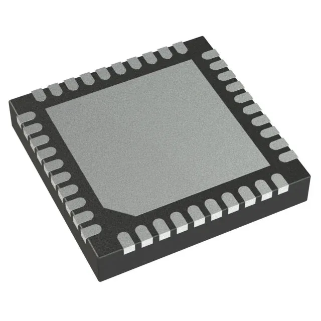
The ADUC7020BCPZ62I is an ARM7TDMI-based MicroConverter from the ADuC7xxx family, clocked at 44 MHz with a 16/32-bit core that executes single-cycle multiply and barrel-shifter operations — the throughput needed for real-time control loops that close around sensor feedback and drive analog outputs on the same die. On-chip data converters include a 5-channel 12-bit ADC and a 4-channel 12-bit DAC, eliminating the need for external converters in precision sensor/actuator chains — a BOM consolidation that matters in space-constrained 40-LFCSP designs. Program memory is 62 KB of Flash (31K x 16) with 2K x 32 of SRAM, providing firmware headroom for moderate-complexity control algorithms, bootloaders, and calibration tables without external memory.
Industrial temperature grade and peripheral set for harsh environments
Peripherals include a programmable logic array (PLA), PWM timer, power-supply monitor (PSM), on-chip temperature sensor, and watchdog timer — the PLA offloads simple glue logic from the core, while the PWM drives motor or heater control directly. Connectivity covers EBI/EMI for external memory or FPGA interface, plus I²C, SPI, and UART/USART serial ports — enough bus headroom to talk to a sensor hub, a serial Flash, and a host controller on the same chip.
Package, supply, and board-fit considerations
Surface-mount only — the 0.50 mm pitch LFCSP demands a solder-paste stencil with 0.25 mm apertures and a reflow profile peaking at 260°C peak per JEDEC J-STD-020 for the RoHS3-compliant assembly.
The 40-LFCSP package is supplied in tray packaging — typical MOQ follows the tray count, confirmed per RFQ.