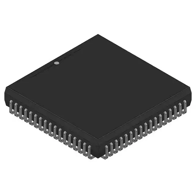
16-bit fixed-point DSP — 68-PLCC, 5 V rails
The ADSP-2115BP-66 is a 16-bit fixed-point digital signal processor from Analog Devices, clocked at 16.67 MHz with 1.5 kB of on-chip RAM and external non-volatile memory support. The 68-PLCC footprint is a legacy workhorse for through-hole reflow or socketed designs — the J-lead form factor gives a visual solder-joint inspection point that BGA lacks, which matters in repair depots that still do visual IPC-610 checks.
Interface and memory architecture
On-chip peripherals include a Host Interface and a Synchronous Serial Port (SSP), giving it a direct path to a host microcontroller or to codec/data converter serial links without external glue logic. The 1.5 kB on-chip RAM is sized for coefficient tables and intermediate buffers in a 16-bit fixed-point algorithm — enough for a 256-tap FIR filter at 16-bit precision, but the algorithm code itself must reside in external non-volatile memory (EPROM or flash) booted via the host or serial port.
Lifecycle and compliance
This part is marked RoHS non-compliant — it was designed before the EU RoHS directive took effect, so it contains lead in the solder plating and possibly in the die attach. For new designs requiring RoHS conformance, a lead-free equivalent (if one exists in the family) must be sourced; for legacy repair or mil/aero contracts that explicitly allow tin-lead, this is the correct BOM line.
Speed-bin comparison within the ADSP-2115 family
The ADSP-2115BP-80 runs at 20 MHz — roughly 20% faster than the -66 bin — and is pin-compatible, making it a drop-in upgrade for designs that can tolerate the higher clock's timing closure and power dissipation. The ADSP-2115BP-40 at 10.24 MHz is the low-power speed grade, useful when the algorithm fits within a longer sample period.