Negative-rail regulation for sensitive analog supplies
The ADP7182ACPZ-5.0-R7 is a negative-output LDO from Analog Devices, delivering a fixed -5 V at up to 200 mA from a maximum input of -28 V. It is built for the negative rail in dual-supply systems — op-amp front ends, ADC reference buffers, or VFD bias circuits that need a clean, low-noise -5 V. Its PSRR profile — 66 dB at 10 kHz rolling to 32 dB at 1 MHz — means it rejects switching-regulator ripple across the audio and low-MHz band, which is where most board-level noise couples into the negative rail. The 0.36 V maximum dropout at full load keeps regulation intact even when the input rail sags close to -5.36 V.
Dropout and quiescent current — what they mean for the rail budget
The 0.36 V dropout at 200 mA sets the minimum headroom: the input must stay below -5.36 V (more negative) to maintain regulation. If the pre-regulator rail is -5.5 V, there is only 0.14 V of margin — a cold-start or load transient that dips the input below -5.36 V will push the output out of spec. Quiescent current is 53 µA typical, rising to 850 µA maximum under full supply. For an always-on negative rail in a battery-powered instrument, that Iq is low enough to avoid a meaningful hit to standby life.
Package and thermal considerations for the 8-LFCSP
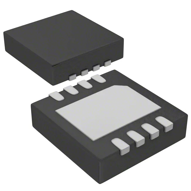
The 8-LFCSP-WD (3x3 mm) exposed-pad package (supplier device package 8-LFCSP-WD) requires a thermal land on the PCB to sink heat. The pad is on the top side — the die attaches directly to it — so the board copper area under the pad sets the junction-to-ambient thermal resistance. For 200 mA at a 5 V drop (1 W dissipation), the pad must connect to a solid ground plane through multiple vias to keep the junction below 125 °C. The enable pin (Control Features: Enable) lets the regulator be shut down externally. When pulled low, the output goes high-impedance and the quiescent current drops to near zero — useful for sequencing the negative rail after the positive rail comes up.
Protection features include over-current and over-temperature shutdown — the regulator folds back output current and latches off if the die exceeds the thermal limit, protecting the load and the board.