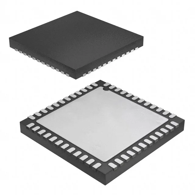
Five-rail power tree in a single 7×7 mm package
The ADP5050ACPZ-R7 integrates four synchronous buck converters and one linear (LDO) regulator into a 48-lead LFCSP with an exposed pad for thermal management — a single-chip solution for multi-rail systems that would otherwise scatter a half-dozen discrete regulators across the board.
Output rail assignment and switching scheme
Output 1 is programmable from 0.85 V to 1.6 V — the core voltage domain for an FPGA or SoC core. Output 2 spans 3.3 V to 5 V, covering the I/O or auxiliary bus. Output 3 delivers 1.2 V to 1.8 V at 1.2 A, typically the DDR memory or PLL supply. All four buck converters switch synchronously at a fixed 740 kHz, which keeps the fundamental switching noise above the audio band and lets the output filter inductor stay in the 1 µH to 4.7 µH range — a practical size for the 48-LFCSP footprint. The part does not include an integrated sequencer, supervisor, or LED driver — sequencing must be handled externally or by a companion power-management IC if the application requires controlled rail ramp-up.
Package, mounting, and thermal path
The 0.5 mm pitch demands a controlled-impedance stack-up for the switching nodes.
Sourcing posture and second-source view
No minimum order quantity is assumed; each RFQ is handled on its own volume. The closest functional peer is the ADP5052ACPZ-R7 — same 4-buck + 1-LDO topology, same 740 kHz switching frequency, same 48-LFCSP package, and the same 4.5 V to 15 V input range. The output 1 voltage range and current ratings differ slightly; verify the rail assignments against the BOM before substituting.