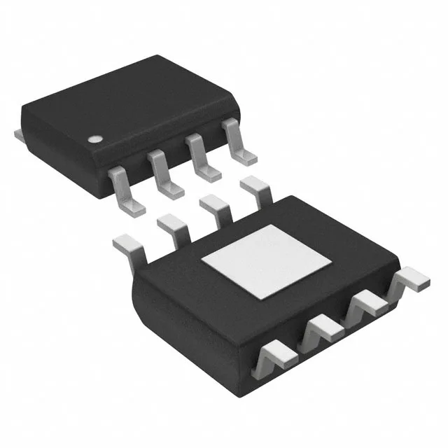
What fits in the kit — package and rework angle
The ADP3624ARDZ-RL comes in an 8-SOIC with an exposed pad — the 0.154-inch wide body is standard SOIC-8 footprint, but that thermal pad underneath means you need a hot-air station or a reflow profile to get the solder wet properly under the die paddle. Hand-soldering the perimeter pins is doable on site if you pre-tin the pad and use a wide tip to heat the tab through the board vias, but the exposed pad is there to pull heat out of the driver, so a cold joint under it will cook the part under continuous 4A switching. It is a surface-mount part, so no socket — you are soldering it down. The 8-SOIC-EP footprint is common enough that most field kits carry a stencil or a pre-formed solder paste dot for the pad. Orientation is obvious: pin 1 is marked with a dot on the package top, and the non-inverting input means the output follows the input without a polarity flip, so a quick continuity check from input to output confirms the part is seated right before power-up.
This is a low-side driver rated for 4A peak source and 4A peak sink — that 4A figure is the peak current the output stage can push into the gate capacitance during switching, not the continuous DC rating. For a typical N-channel MOSFET with 10 nC of gate charge, a 4A drive current means the gate voltage slews from 0 to 10V in about 2.5 ns, which is well within the 10ns typical rise time the datasheet guarantees. The supply range runs from 4.5V to 18V, so it works off a standard 12V rail or a 5V logic supply. The logic thresholds are 0.8V for VIL and 2V for VIH — that means a 3.3V microcontroller output with a 0.4V low and 3.0V high has enough margin to drive the input directly without a level shifter. The two drivers are independent and non-inverting — each channel has its own input pin and drives its own output. This lets you drive two separate MOSFETs with independent PWM signals, or parallel the outputs for higher peak current into a single large gate. The 10ns rise and fall times are symmetric, so the dead-time between high-side and low-side switching in a half-bridge is determined by your PWM timing, not by the driver asymmetry.