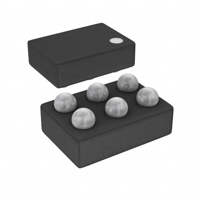
12 mOhm Rds(on) — conduction loss floor for a 3 A rail
The ADP197ACBZ-01-R7: At 3 A continuous output, that translates to roughly 108 mW of I²R loss at 25 °C — low enough that the WLCSP package's thermal path to the board, not the silicon, sets the current ceiling. The On/Off control input is non-inverting: logic high turns the pass FET on.
Slew-rate control and fault protection
The slew-rate controlled turn-on limits inrush current into capacitive loads — a feature that matters when the switch powers a downstream DC-DC converter or a bank of decoupling capacitors that would otherwise pull a current spike on hot-plug. The part includes over-temperature fault protection that shuts off the FET if the die exceeds the thermal threshold.
WLCSP-6 footprint — board integration demands
The 6-WFBGA WLCSP package measures 1.45 mm x 0.95 mm (supplier device package 6-WLCSP). This is a wafer-level chip-scale package with solder bumps directly on the die pads — no mold compound. The board footprint must match the ball layout exactly; the 0.4 mm pitch typical of this class demands a soldermask-defined pad and a stencil aperture sized for the bump diameter. No exposed thermal pad — heat sinks through the solder balls into the PCB copper. The RoHS3 compliance covers the entire bill of materials including the solder ball metallurgy.