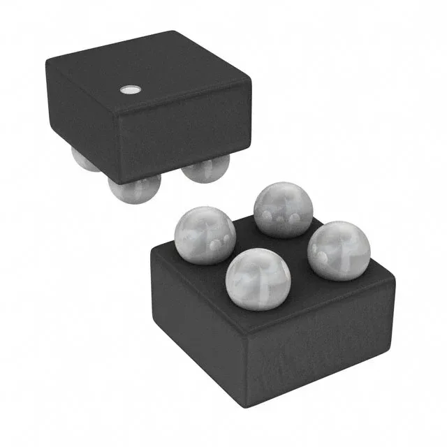
Analog Devices ADP150ACBZ-3.0-R7 — Power Management (PMIC / Gate Driver)

ADP150ACBZ-3.0-R7 LDO 3V 150mA 4-WLCSP

MPNADP150ACBZ-3.0-R7
End of Life

Analog Devices ADP150ACBZ-3.0-R7, fixed-output LDO, 3V, 150mA, 4-WFBGA WLCSP, tape and reel.

$1.4Ref. price · indicative, final on quote
Packaging4-WFBGA, WLCSP
RoHSROHS3 Compliant
Sourced new & surplus through independent channelsAuthenticity-screened · ESD-safe packingListing updated Aug 2026

Specifications

ADP150ACBZ-3.0-R7 specifications
ParameterValue
Output typeFixed
MountingSurface Mount
Voltage - input5.5V
Voltage dropout0.16V @ 150mA
Voltage - output (Min (Fixed))3V
Output current150mA
Current - supply320 µA
Current - quiescent22 µA
Operating temperature-40°C ~ 125°C
PackageTape & Reel (TR); Cut Tape (CT)
Case4-WFBGA, WLCSP
Control featuresEnable
Protection featuresOver Current, Over Temperature, Under Voltage Lockout (UVLO)
Number of regulators1
Output configurationPositive

Product details

3V fixed rail with 150mA headroom

The ADP150ACBZ-3.0-R7 is a fixed 3V positive-output LDO regulator delivering up to 150mA continuous current from a 2.2V to 5.5V input rail. Maximum dropout is 160mV at the full 150mA load, meaning the input must stay above 3.16V across the load range to maintain regulation — a 3.3V rail with 5% tolerance (3.135V min) would risk dropout at high current; a 3.6V or 5V rail provides comfortable margin.

Quiescent budget and thermal envelope

Quiescent current is 22µA typical, rising to a maximum supply current of 320µA — this places the regulator in the low-Iq class suited for always-on sensor nodes or battery-backed domains where the LDO's own draw must not dominate the sleep budget. The 4-WLCSP package (0.76x0.76mm body) has a thermal resistance dictated by the board copper area under the bump array — the junction-to-ambient path is through the PCB, not a heatsink tab. Built-in protection includes over-current, over-temperature, and under-voltage lockout (UVLO) — the UVLO threshold prevents the pass element from operating in the linear region when the input rail sags, avoiding excessive dissipation.

Frequently asked questions

What package does ADP150ACBZ-3.0-R7 use?

4-ball WLCSP (Wafer-Level Chip Scale Package) with a 0.76x0.76mm body, 0.50mm ball pitch. The supplier device package code is 4-WLCSP (0.76x0.76).

What protection features are included?

Over-current, over-temperature, and under-voltage lockout (UVLO). The UVLO disables the output when the input voltage drops below the minimum operating threshold, preventing the pass FET from entering the linear region.