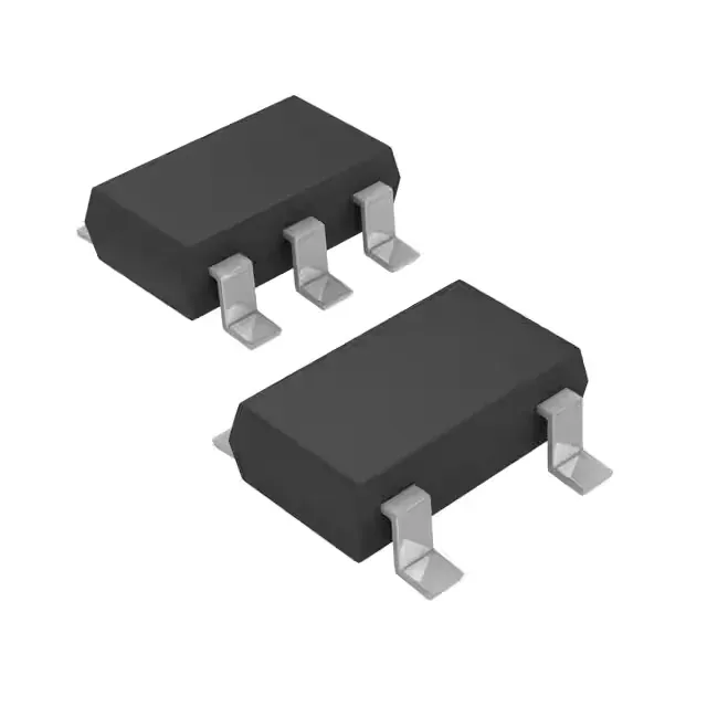
1.2V rail at 350mA — the core-supply or I/O regulator that sits between a noisy buck and a sensitive load
The ADP130AUJZ-1.2-R7 is a fixed 1.2V output LDO rated for 350mA continuous — enough to power a small FPGA core rail, a wireless SoC's digital supply, or a set of sensor front-ends from a single 3.6V max input bus. Quiescent current sits at 44 µA typical, with a maximum supply current of 220 µA — the idle draw is low enough that the regulator doesn't dominate the battery budget in always-listening IoT endpoints. The PSRR profile — 70 dB at 10 kHz rolling to 54 dB at 100 kHz — tells you where this part earns its keep: cleaning up the switching ripple from a preceding buck converter that operates in the tens to low hundreds of kilohertz.
PSRR across frequency — what the 70dB-to-54dB slope means on a real board
At 10 kHz the regulator rejects 70 dB of input ripple — that's a 3162× attenuation, so a 100 mVpp switching artifact on the input rail becomes roughly 32 µVpp at the output. By 100 kHz the rejection drops to 54 dB (501× attenuation) — the same 100 mVpp input ripple now appears as 200 µVpp at the output. If the downstream load is a 1.2V ADC reference or a PLL supply, that 200 µVpp may still be within the noise budget; if the load is a precision analog front-end, you'll want an additional LC filter ahead of the LDO. The -40°C to 125°C operating range means the PSRR and dropout characteristics hold across industrial and automotive ambient conditions — the 125°C ceiling covers under-hood engine-bay air without derating the output current.
Package and board-fit — TSOT-23-5 footprint and thermal reality
The part comes in a TSOT-23-5 — a 5-lead thin SOT with a 0.95 mm pitch. The footprint matches a standard SOT-23-5 land pattern, but the package height is lower, which helps in stacked-board assemblies or under-shielding cans. At 350 mA output with a 1.2V drop from a 2.5V input (0.455 W dissipation), the TSOT-23-5's junction-to-ambient thermal resistance of roughly 230°C/W means the die sits about 105°C above ambient — well within the 125°C maximum junction temperature at 25°C ambient, but tight at 85°C ambient. A small copper pour on the PCB's top layer under the package drops that thermal resistance by 20–30%.
Protection set and control — three failure modes this LDO handles without a discrete supervisor
Over-current, over-temperature, and under-voltage lockout (UVLO) are all on-chip — the regulator shuts itself down before a shorted load or a drooping input rail takes out the downstream circuitry. The UVLO threshold prevents the pass transistor from operating in the linear region where dissipation spikes. The Enable pin lets a GPIO or a power sequencer turn the output on and off — useful for sequencing multiple rails or gating power to a sleep-mode load. When disabled, the output goes high-impedance, not pulled to ground.
Active lifecycle and compliance — no end-of-life watch needed
ROHS3 compliant — no restricted substances above the exemption thresholds, which simplifies EU and California regulatory acceptance.