Switch parametrics and load fit
The ADP1196ACBZ-02-R7 is a single-channel, N-channel power switch rated for 3 A continuous output with a typical on-resistance of 10 mOhm. The Rds(on) at this level means conduction loss at 3 A is under 90 mW — negligible for most board-level power routing, but the WLCSP package's thermal path to the board should be considered for sustained full-load operation above 85 °C. It operates from a load voltage of 1.83 V to 5.5 V and can be configured as a high-side or low-side switch. The input type is non-inverting with a simple On/Off interface, and no external Vcc/Vdd supply is required — the switch is self-powered from the load rail.
Protection and control features
Built-in fault protection includes fixed current limiting and over-temperature shutdown. The current limit is factory-set and not adjustable — the 3 A max rating is the absolute ceiling, and the limit engages before the die reaches the thermal shutdown threshold. For loads that draw near the limit, the designer should budget for the foldback characteristic in the datasheet's typical-performance curves. Slew-rate controlled switching prevents inrush current from causing the upstream rail to droop when the switch turns on. This is particularly relevant when the load includes bulk decoupling capacitance — the controlled turn-on avoids a voltage dip that could reset co-mounted logic.
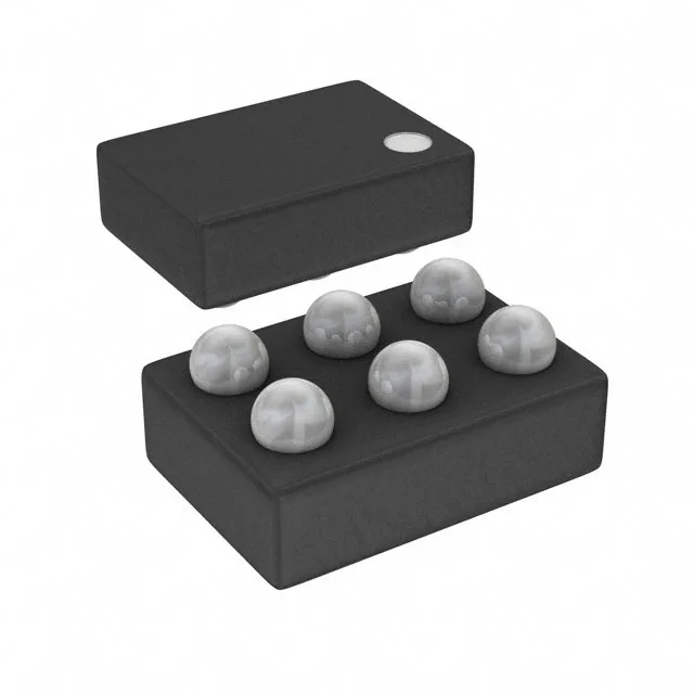
Housed in a 6-ball WLCSP measuring 1.45 x 0.95 mm (supplier device package 6-WLCSP). The 0.4 mm ball pitch is typical for this class of CSP — the footprint requires a solder-mask-defined pad with a non-solder-mask-defined opening for reliable ball attach. A 0.35 mm pad diameter on a 0.4 mm pitch leaves 0.05 mm clearance, which is within standard PCB fab capability for a 4-layer board. The WLCSP's junction-to-board thermal resistance is dominated by the copper pad area under the balls; a solid via array under the package drops RthJB significantly.
Lifecycle and compliance
The Tape & Reel packaging (7-inch reel, 3000 pieces per reel) is the standard procurement unit for this WLCSP. The closest parametric peers are the ADP196ACBZ-R7, ADP196ACPZN-R7, and ADP196ACPZN-01-R7 — all share the same 10 mOhm Rds(on), 3 A output, same fault protection set, and same temperature grade. The ADP196ACPZN-01-R7 adds a load-discharge feature (active pull-down when disabled) that the ADP1196 lacks. The primary difference is package: the ADP1196 uses the smaller WLCSP (1.45 x 0.95 mm), while the ADP196 variants use either WLCSP or LFCSP. A board laid out for the WLCSP footprint cannot accept an LFCSP without a layout change.