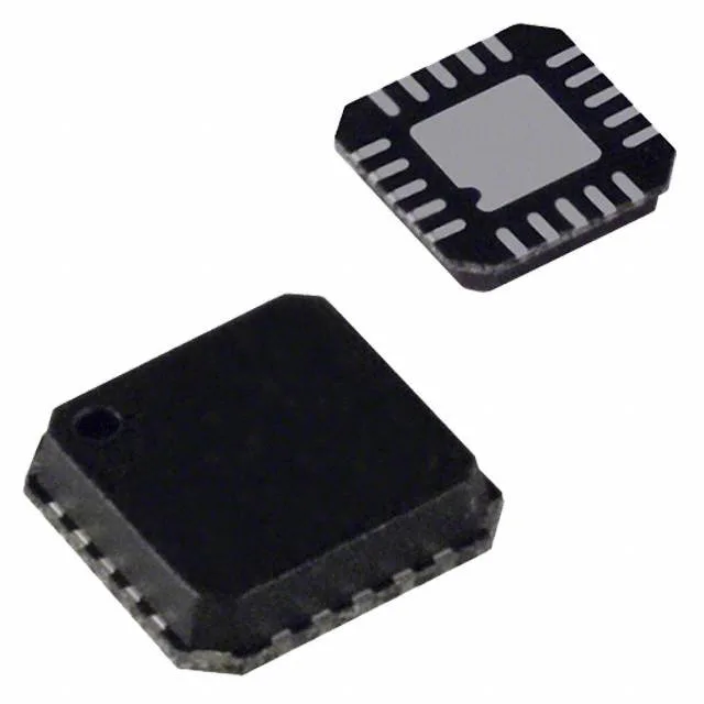
Active quad SPDT — 900 MHz bandwidth, 0.5 pC injection
The ADG1234YCPZ-REEL7: The -3 dB bandwidth of 900 MHz means this switch passes high-frequency signals — video, RF up to UHF, or fast digital data — with minimal roll-off. The -85 dB crosstalk at 1 MHz tells you adjacent channels stay isolated; a signal on one path leaks less than 0.006% into the neighbouring channel, which matters for precision analog multiplexing or multi-channel data acquisition. Charge injection is rated at 0.5 pC typical. That is the tiny packet of charge the switch dumps onto the output when it toggles. In a sample-and-hold or a DAC output multiplexer, 0.5 pC into a 10 pF hold capacitor creates a 50 mV glitch — small enough to settle before the next conversion cycle in most 12-bit systems.
Package, supply, and temperature — what fits the board
Housed in a 20-lead LFCSP (4x4 mm) with an exposed pad — the 20-WFQFN package variant. The pad also gives you a solid mechanical anchor during rework — a hot-air station at 300°C with a fine nozzle lifts the part cleanly if you preheat the board from the bottom to 100°C first. Supply range covers single 5 V to 16.5 V or dual ±5 V to ±16.5 V. The 190-ohm max on-resistance is specified at 25°C with a ±15 V supply — it rises with temperature and drops as supply voltage increases. Channel-to-channel matching of 3.5 ohm means the four switches track each other within that spread, important for gain-matching in a multiplexed PGA front-end. The switch time (140 ns on, 45 ns off) is specified at 25°C with a 5 V supply; expect it to slow by roughly 20% at 125°C and speed up slightly at cold. The 100 pA max off-leakage and 1.7/1.8 pF channel capacitance keep the signal path clean at high impedance.
Sourcing and compliance — active, RoHS3, reel
The closest functional peer is the ADG1234YRUZ-REEL7 — same die, same quad SPDT topology, same 900 MHz bandwidth and -85 dB crosstalk, but packaged in a 20-TSSOP instead of the LFCSP. The pinout differs between the two packages, so a board spin is required to swap them. The ADG1233YCPZ-REEL7 is a triple (3-circuit) version in the same LFCSP footprint, useful if one channel is unused.