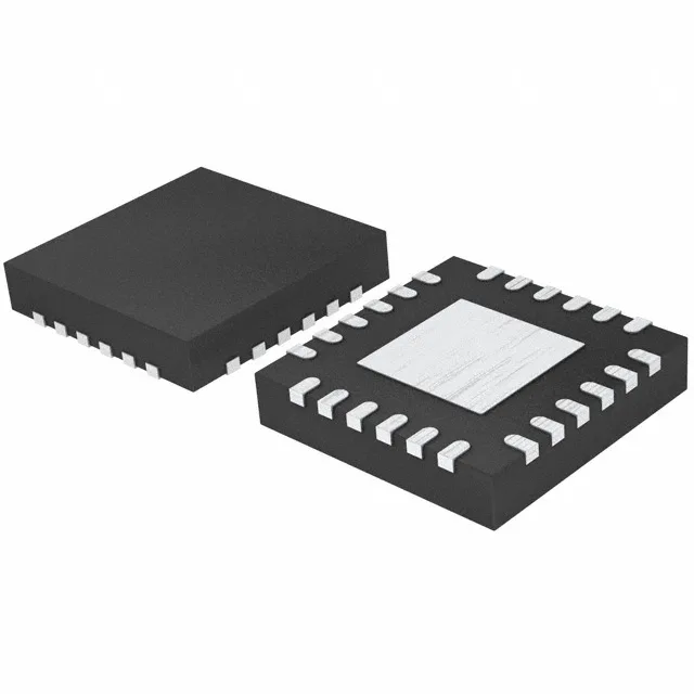
Analog Devices ADF4360-1BCPZRL7 — Analog & Data Acquisition

ADF4360-1BCPZRL7 PLL Synthesizer, 2.45 GHz, 24-LFCSP

MPNADF4360-1BCPZRL7
End of Life

Analog Devices ADF4360-1BCPZRL7, Integer N Synthesizer (RF) with PLL, Fanout Distribution, 1 circuit, 1:2 input:output ratio, CMOS/TTL input, Clock output, 2.45 GHz max frequency, 3V to 3.6V supply, -40°C to 85°C, 24-LFCSP (4x4) surface mount.

$10.04Ref. price · indicative, final on quote
Packaging24-WFQFN Exposed Pad, CSP
StockContact for availability
MOQ1 pcs
  • 100% new & originalTraceable channels only — no refurbs, no pulls, no remarked parts.
  • Date & lot codes on quoteStated per line before you commit; label photos on request.
  • MSL-compliant ESD packingMoisture-sealed bags with indicator cards; reels photo-verified.
  • PayPal buyer protectionPay by T/T, PayPal or Payoneer — card payments covered end to end.

Specifications

ADF4360-1BCPZRL7 Technical Specifications
ParameterValue
TypeFanout Distribution, Integer N Synthesizer (RF)
Mounting typeSurface Mount
Voltage3V ~ 3.6V
Frequency2.45GHz
Operating temperature-40°C ~ 85°C
PLLYes
InputCMOS, TTL
OutputClock
PackageTape & Reel (TR); Cut Tape (CT)
Case24-WFQFN Exposed Pad, CSP
Divider (Multiplier)Yes/No
Number of circuits1
Ratio - Input:Output1:2
Differential - Input:OutputNo/No

Product details

What the ADF4360-1BCPZRL7 is and where it fits

The Analog Devices ADF4360-1BCPZRL7 is an integer-N synthesizer with integrated VCO, combining a PLL core and voltage-controlled oscillator in a single 24-LFCSP package. It accepts CMOS or TTL reference inputs and delivers a clock output, making it a compact frequency source for RF upconversion, local oscillator generation, and clock distribution in wireless infrastructure, test equipment, and microwave backhaul links.

2.45 GHz maximum frequency — what it means for the signal chain

The 2.45 GHz upper limit places this part in the 2.4 GHz ISM band and lower microwave range, suitable for WLAN, Bluetooth, Zigbee basestation local oscillators, and point-to-point radio IF stages. The integer-N architecture means the loop filter and reference must be chosen to hit the exact output frequency; fractional-N parts cover finer step sizes but this one trades that for lower in-band phase noise typical of integer-N designs. The 1:2 input-to-output ratio lets a single reference feed two synthesizer paths or fan out to a second stage without an external buffer.

3V to 3.6V supply — rail design and decoupling

The supply window is tight at 3V to 3.6V, so a 3.3V rail with ±5% tolerance keeps the part inside spec. The integrated VCO draws significant current during lock acquisition; a low-ESR 10 µF ceramic plus a 100 nF per supply pin, placed within 2 mm of each pin, is the standard decoupling recipe for the 24-LFCSP package. The exposed pad (pin 0) must be soldered to a ground plane with thermal vias — the datasheet's recommended footprint is a 4x4 array of 0.3 mm vias under the pad to keep the junction temperature in check during continuous operation at 85°C ambient.

Industrial temperature range and package handling

Rated -40°C to 85°C, this part suits outdoor telecom cabinets, industrial RF transceivers, and automotive test equipment that sees under-hood temperature swings. The 24-LFCSP (4x4 mm) is a leadless package with a 0.5 mm pitch — reflow profile per JEDEC MSL 3 applies; if the moisture barrier bag has been open longer than 168 hours at <30°C/60% RH, bake at 125°C for 48 hours before reflow. The exposed pad is the primary thermal path; a poor solder joint there will cause frequency drift or loss of lock at high temperature.

Frequently asked questions

Will ADF4360-1BCPZRL7 drop into a board designed for ADF4360-1BCPZ?

Yes — the two parts share the same die, electrical specifications, and 24-LFCSP package. The only difference is the shipping medium: the -1BCPZRL7 comes on Tape & Reel, while the -1BCPZ ships in Tray. No layout or BOM change is needed.