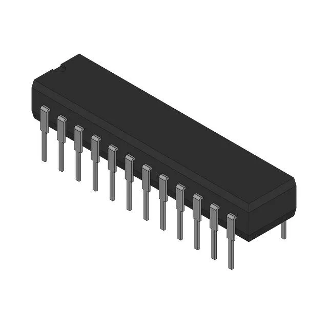
Analog Devices ADDAC80-CBI-I — Discrete Semiconductors

ADDAC80-CBI-I 12-bit DAC, 4µs settling, CDIP-24

MPNADDAC80-CBI-I
End of Life

ADDAC80-CBI-I 12-bit DAC, current-buffered output, 4µs settling time, ±0.5 LSB INL/DNL, parallel interface, CDIP-24 package, through-hole mounting.

$57.2Ref. price · indicative, final on quote
Packaging24-CDIP (0.600", 15.24mm)
RoHSRoHS non-compliant
Sourced new & surplus through independent channelsAuthenticity-screened · ESD-safe packingListing updated Aug 2026

Specifications

ADDAC80-CBI-I specifications
ParameterValue
Output typeCurrent - Buffered
MountingThrough Hole
Reference typeExternal, Internal
Voltage - supply, analog±11.4V ~ 16.5V
Voltage - supply, digital±11.4V ~ 16.5V
InterfaceParallel
Operating temperature-25°C ~ 85°C
PackageBulk
INL (DNL)±0.5, ±0.5
Settling time4µs
Number of bits12
Case24-CDIP (0.600\", 15.24mm)
Differential outputNo
Number of d (A converters)1

Product details

12-bit DAC with 4 µs settling in a hermetic CDIP-24

The ADDAC80-CBI-I is a 12-bit digital-to-analog converter with a current-buffered output, settling to within ±0.5 LSB in 4 µs. It accepts parallel data and provides a current output that can be converted to voltage with an external op-amp. Housed in a 24-pin ceramic DIP (0.600-inch body width), it is a through-hole part suited for legacy or high-reliability board builds where a hermetic package is preferred.

Supply rails and reference flexibility

The part operates on analog and digital supplies of ±11.4 V to ±16.5 V, and accepts either an external or internal voltage reference. The dual-supply requirement means the board must provide both positive and negative rails — a single-supply system will not work without a DC-DC converter.

Active lifecycle and compliance status

Note that the part is RoHS non-compliant. For builds requiring RoHS exemption or lead-free assembly, a different DAC variant or a secondary source such as the AD667AD (also through-hole, 12-bit, 4 µs settling) should be evaluated. The AD667AD is a voltage-output device, so the output stage differs, but the digital interface and resolution match.

Sourcing and supply posture

As an active part with no single-source restriction, the ADDAC80-CBI-I can be quoted to order through independent distribution. For BOM risk management, the AD667AD offers a drop-in functional alternative in the same package and pinout, though its output is voltage-buffered rather than current-buffered. Verify the downstream circuit's input impedance before substituting.

Frequently asked questions

What is the closest functional second-source for ADDAC80-CBI-I?

The AD667AD is a close functional match — same 12-bit resolution, 4 µs settling time, parallel interface, and through-hole CDIP package. The key difference is output type: AD667AD provides a voltage-buffered output versus the ADDAC80-CBI-I's current-buffered output. Verify the load circuit before substituting.

What compliance documentation does ADDAC80-CBI-I carry?

The part is RoHS non-compliant. For RoHS-exempt or lead-free builds, an alternative DAC should be sourced.

How can I order ADDAC80-CBI-I or check availability?

The ADDAC80-CBI-I is sourced to order through independent distribution.