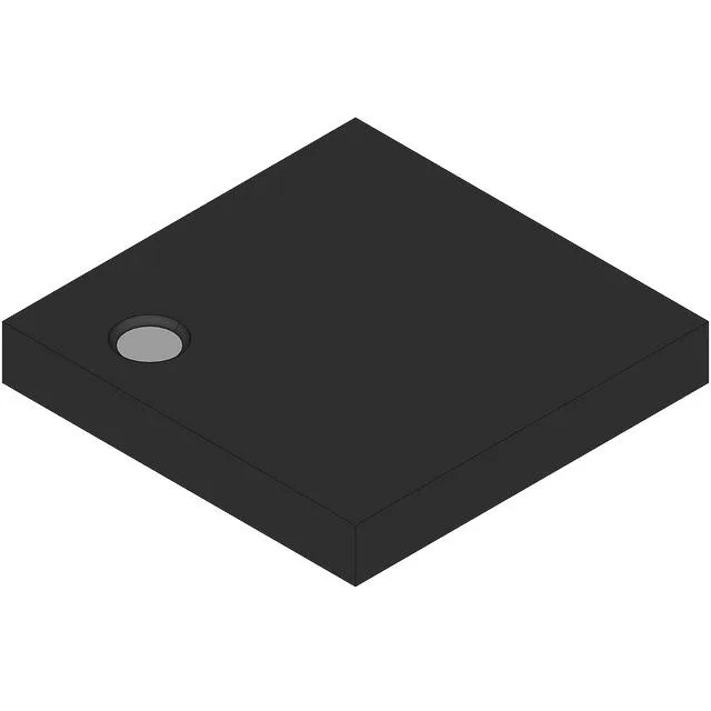
Analog Devices ADCMP563BCPZ-WP — Analog & Data Acquisition

ADCMP563BCPZ-WP Dual Comparator, 0.83 ns, Latch, LFCSP

MPNADCMP563BCPZ-WP
End of Life

Analog Devices ADCMP563 series, Dual Comparator with Latch, 0.83 ns propagation delay, 80 dB CMRR, 85 dB PSRR, 16-LFCSP-WQ (3x3 mm), Surface Mount, Bulk.

$3.52Ref. price · indicative, final on quote
Packaging16-WFQFN Exposed Pad, CSP
SeriesADCMP563
Sourced new & surplus through independent channelsAuthenticity-screened · ESD-safe packingListing updated Aug 2026

Specifications

ADCMP563BCPZ-WP specifications
ParameterValue
Typewith Latch
SeriesADCMP563
Output typeComplementary, -
MountingSurface Mount
Voltage - input offset10mV @ 5V
Voltage - supply, single (Dual (±))4.75V ~ 5.25V, ±2.375V ~ 2.625V
Output current30mA
Current - quiescent5mA, 25mA
Current - input bias10µA @ 5V
Operating temperature-40°C ~ 85°C
PackageBulk
Hysteresis±1mV
Case16-WFQFN Exposed Pad, CSP
CMRR, PSRR80dB CMRR, 85dB PSRR
Number of elements2
Propagation delay0.83ns

Product details

Key parametric decisions for the comparator selection

The ADCMP563BCPZ-WP: With a 0.83 ns maximum propagation delay, this dual comparator resolves input differences fast enough for high-speed threshold detection, clock recovery, or zero-crossing circuits where timing margin is tight. The latch function (Type: with Latch) holds the output state after the compare strobe, which is essential in sampled-data systems — the comparator captures the input level at a specific clock edge and retains it until the next latch enable. Typical CMRR of 80 dB and PSRR of 85 dB mean the comparator rejects common-mode noise on the inputs and supply ripple, maintaining threshold accuracy in noisy industrial or mixed-signal environments.

Package and board-fit note

Housed in a 16-lead LFCSP-WQ (3x3 mm) with exposed pad — the thermal pad should be soldered to a PCB copper plane for adequate heat dissipation, especially when both comparators are switching at speed.

Complementary outputs and input characteristics

Complementary output type provides both in-phase and inverted signals — useful for driving differential lines or feeding a latch input and its complement without external inversion. Maximum input bias current of 10 µA at 5 V and input offset voltage of 10 mV at 5 V define the DC accuracy floor; for precision threshold applications, account for these offsets in the trip-point calculation. Each output can sink or source 30 mA typical, enough to drive a standard logic gate input or a small LED indicator directly.

Frequently asked questions

What is the closest functional alternative to ADCMP563BCPZ-WP?

The ADCMP562BRQZ shares the same 0.83 ns propagation delay, ±1 mV hysteresis, 80 dB CMRR, and dual-comparator architecture, but comes in a 16-lead QSOP package with complementary differential PECL outputs rather than the LFCSP. The pinout and output standard differ, so a board respin is required for a direct swap.

What compliance documentation does Analog Devices provide for ADCMP563BCPZ-WP?

Analog Devices typically provides RoHS and REACH compliance declarations for this part. No UL or IEC certification is listed in the available specifications.