Analog Devices ADCLK946BCPZ — Clock & Timing ICs

ADCLK946BCPZ Clock Buffer 1:6 4.8GHz LVPECL Analog Devices

MPNADCLK946BCPZ
End of Life

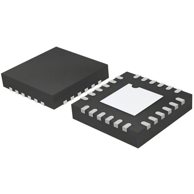
Analog Devices ADCLK946BCPZ, SiGe Fanout Buffer (Distribution), 1:6 ratio, 4.8 GHz max frequency, LVPECL output, 24-LFCSP-VQ (4x4) package, industrial temperature range -40°C to 85°C.

$12.27Ref. price · indicative, final on quote
Packaging24-VFQFN Exposed Pad, CSP
StockContact for availability
MOQ1 pcs
  • 100% new & originalTraceable channels only — no refurbs, no pulls, no remarked parts.
  • Date & lot codes on quoteStated per line before you commit; label photos on request.
  • MSL-compliant ESD packingMoisture-sealed bags with indicator cards; reels photo-verified.
  • PayPal buyer protectionPay by T/T, PayPal or Payoneer — card payments covered end to end.

Specifications

ADCLK946BCPZ Technical Specifications
ParameterValue
TypeFanout Buffer (Distribution)
SeriesSiGe
Mounting typeSurface Mount
Voltage2.97V ~ 3.63V
Frequency4.8 GHz
Operating temperature-40°C ~ 85°C
InputCML, CMOS, LVDS, LVPECL
OutputLVPECL
PackageTray
Case24-VFQFN Exposed Pad, CSP
Number of circuits1
Ratio - Input:Output1:6
Differential - Input:OutputYes/Yes

Product details

4.8 GHz clock distribution in a 24-LFCSP footprint

The ADCLK946BCPZ is a 1:6 fanout buffer from Analog Devices' SiGe series, rated for a maximum frequency of 4.8 GHz. It accepts CML, CMOS, LVDS, or LVPECL inputs and delivers LVPECL outputs — so the same buffer can sit behind a PLL output or a crystal oscillator without needing a translator.

Supply range and signal compatibility

Supply voltage range is 2.97 V to 3.63 V, which aligns with a 3.3 V rail ±10 %. The differential input and output path means the buffer rejects common-mode noise on the clock trace — important when the source and load are on different boards connected by a cable. Compared to the ADCLK948BCPZ (2:8 fanout/mux) or ADCLK950BCPZ (2:10), this 1:6 part is the simpler fanout-only choice when you do not need input selection.

Layout and thermal considerations

The 24-VFQFN exposed-pad CSP requires a solder-paste stencil opening that covers at least 50 % of the pad area to avoid voids. The exposed paddle is the primary thermal path — connect it to a solid ground plane with at least four thermal vias under the pad. The 4.8 GHz bandwidth supports 10-GbE reference clocks and ADC sampling clocks without edge degradation.

Frequently asked questions

What is the difference between ADCLK946BCPZ and ADCLK948BCPZ?

The ADCLK946BCPZ is a 1:6 fanout buffer, while the ADCLK948BCPZ is a 2:8 fanout buffer with an integrated input multiplexer. They are not pin-compatible — the 948 adds a second input and two more outputs.