7.5 GHz clock buffer — active production
The ADCLK914BCPZ-R2 is an Analog Devices SiGe clock buffer/driver rated for a maximum frequency of 7.5 GHz. This bandwidth places it in the class of parts used for high-speed ADC clock conditioning, SERDES reference distribution, and RF test equipment clock trees where signal integrity at multi-GHz rates is non-negotiable.
Input flexibility and supply rails
The buffer accepts CML, CMOS, LVDS, LVPECL, and LVTTL input levels — a single BOM position that can bridge across logic families in a mixed-signal board. The output is HVDS, a differential standard that keeps edge rates clean over short PCB traces to the downstream load. Supply voltage range is 2.97 V to 3.63 V, which aligns with common 3.3 V rails.
The ADCLK914BCPZ-R2 is the 250-piece reel variant; the same die and package are also available as ADCLK914BCPZ-R7 (500-piece reel). Sourcing is confirmed per RFQ — no stock-holding claim, but the part is in current manufacture so lead time follows Analog Devices' standard production cycle. Date-code provenance is straightforward for an active part; no mystery stock concerns.
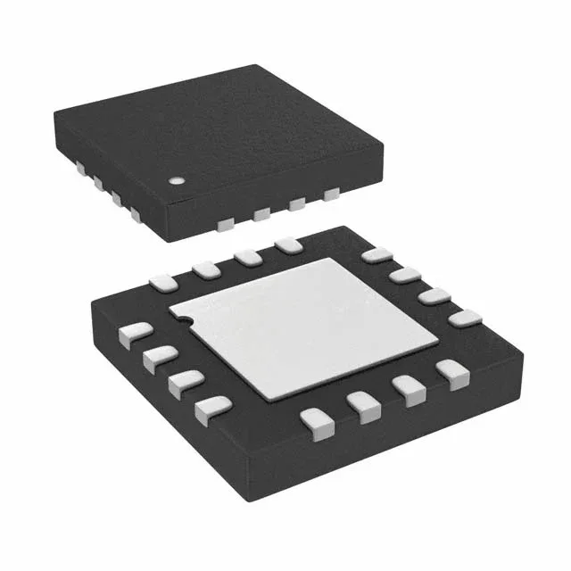
Package is 16-VFQFN Exposed Pad, CSP, also designated 16-LFCSP-VQ (3x3). Surface-mount mounting with a tape-and-reel carrier — the R2 suffix indicates 250 pieces per reel, which is a smaller quantity than the R7 variant's 500-piece reel. For prototype or low-volume builds, the R2 reel avoids excess inventory.