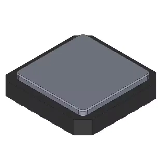
Analog Devices AD9768SE — Discrete Semiconductors

AD9768SE Multiplying DAC, 8-Bit, 5ns Settling, 20-CLCC

MPNAD9768SE
End of Life

Analog Devices AD9768SE Multiplying DAC, 8-bit, current-buffered output, 5ns settling time, parallel interface, 20-CLCC package, -55°C to 125°C operating range.

$27.6Ref. price · indicative, final on quote
Packaging20-CLCC
RoHSRoHS non-compliant
SeriesAD9768
Sourced new & surplus through independent channelsAuthenticity-screened · ESD-safe packingListing updated Aug 2026

Specifications

AD9768SE specifications
ParameterValue
SeriesAD9768
Output typeCurrent - Buffered
MountingSurface Mount
Reference typeExternal
InterfaceParallel
Operating temperature-55°C ~ 125°C
PackageBulk
ArchitectureMultiplying DAC
Settling time5ns
Number of bits8
Case20-CLCC
Differential outputNo
Number of d (A converters)1

Product details

5 ns settling — the speed axis for this multiplying DAC

The AD9768SE is an 8-bit multiplying DAC from the AD9768 series, delivering a current-buffered output with a 5 ns settling time. That settling figure — 5 ns to within 1/2 LSB — sets the update rate ceiling: with a parallel interface, the data bus must present a new word and hold it long enough for the internal current switches to settle before the next strobe. For a multiplying DAC, the reference input can be modulated at speed, so the 5 ns spec governs both the digital word update and the analog reference bandwidth.

Military temperature grade and hermetic package

Rated for -55°C to 125°C operating temperature, the AD9768SE spans the full military temperature band. The 20-CLCC package (ceramic leadless chip carrier) with a 9x9 mm 20-LCCC footprint provides a hermetic seal — moisture ingress is blocked, so the die sees no humidity-driven corrosion or parametric drift over decades of storage or cycling. This combination targets avionics, satellite payloads, and downhole instrumentation where the board must survive thermal shock and vacuum without outgassing. The multiplying DAC architecture accepts an external reference — the reference input doubles as a second signal input, so the output is the product of the digital code and the analog reference voltage. With no differential output, the single-ended current output drives into a transimpedance amplifier or directly into a summing node. The parallel data interface writes all 8 bits simultaneously, which is the fastest way to load a new code when the bus width matches.

Active lifecycle and compliance posture

Note that the RoHS compliance status is listed as non-compliant, which is expected for a hermetic ceramic package containing lead-based solder seals; this part is exempt from RoHS restrictions for military/aerospace applications under the exemption for high-reliability solders.

Frequently asked questions

What is the AD9768SE's settling time and what does it mean for my design?

The AD9768SE settles to within 1/2 LSB in 5 ns. This is the time from a digital code transition on the parallel bus until the analog output reaches its final value within the specified error band. For a multiplying DAC, this settling time applies to both the digital word update and the analog reference modulation — the reference input can be driven with signals up to the bandwidth implied by the 5 ns step response. The parallel interface writes all 8 bits simultaneously, so the bus cycle must allow at least 5 ns between writes for the output to settle.

Can the AD9768SE replace the AD5341BRUZ-REEL7 in an existing design?

No, these are not drop-in replacements. The AD9768SE is an 8-bit multiplying DAC with a current-buffered output and 5 ns settling time in a 20-CLCC hermetic package, while the AD5341BRUZ-REEL7 is a 12-bit string DAC with a voltage-buffered output and 10 µs settling time in a surface-mount plastic package. The architecture, resolution, settling speed, output type, and package are all different — a board spin would be required to swap between them.