12-bit update rate and linearity for waveform generation
The AD9712BBP is a 12-bit digital-to-analog converter with a 27 ns settling time — the output settles to within 1/2 LSB in 27 ns, so the maximum update rate is roughly 37 MHz for a full-scale step. That puts it in the range for direct-digital-synthesis (DDS) waveform generation up to several MHz, or for arbitrary-function generators where the clock drives the DAC at its full rate. Integral nonlinearity is ±1 LSB and differential nonlinearity is ±1.25 LSB — the spurious-free dynamic range (SFDR) at moderate update rates is dominated by these static errors, not by glitch energy. For a 12-bit system, ±1 LSB INL means the transfer curve stays within one code width of ideal, which is typical for a segmented R-2R architecture.
Current-source R-2R with buffered output
The architecture is a current-source R-2R network with a buffered current output — the output is a current proportional to the digital code, not a voltage. That means the load resistor sets the voltage swing; a 50-ohm load gives a 0 to -0.5 V swing for a 10 mA full-scale current. The output is not differential, so a single-ended op-amp stage after the DAC is the usual interface for driving a 50-ohm back-terminated cable. The reference can be external or internal — if the system already has a precision voltage reference, the internal reference can be bypassed to save power. The internal reference is trimmed for the full-scale current, but an external reference lets you scale the output range independently of the DAC code.
28-PLCC J-lead — socket or rework
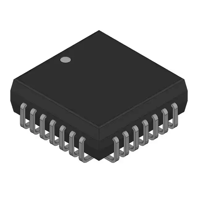
The package is a 28-lead PLCC with J-leads (28-LCC J-Lead), body size 11.51 mm square. The J-lead profile means the part sits flush against the board — no standoff — and the leads are hidden under the body. On a rework station, a hot-air nozzle with a 12 mm square aperture works; the part lifts off cleanly when the solder under all four sides is molten. A PLCC extraction tool helps avoid lifting pads. Surface-mount soldering profile: the J-lead pads are on a 1.27 mm pitch, so standard fine-pitch solder paste works. No special moisture sensitivity level is stated in the listing — assume MSL 3 or higher unless the part has been baked before reflow. The operating temperature range is -25°C to 85°C, which covers most industrial test equipment and ATE environments but not extended automotive or military.