Quad JFET op-amp for precision analog front-ends
It combines a 3.5 MHz gain-bandwidth product with a 3V/µs slew rate, rail-to-rail output swing, and an input bias current of 0.25 pA.
The 0.25 pA typical input bias current is the standout parameter here. For a photodiode amplifier or a high-impedance sensor bridge, that leakage floor determines the minimum detectable signal. A CMOS-input op-amp might claim similar bias, but the JFET architecture also keeps voltage noise low at higher source impedances. The 70 µV input offset voltage is respectable for a general-purpose precision part — not the sub-10 µV class of auto-zero amplifiers, but well within what a 12-bit or 14-bit ADC driver needs after a gain stage.
Rail-to-rail output and supply range
The rail-to-rail output swings close to the supply rails. Supply range spans 5 V minimum to 26 V maximum. Each channel sources or sinks 12 mA.
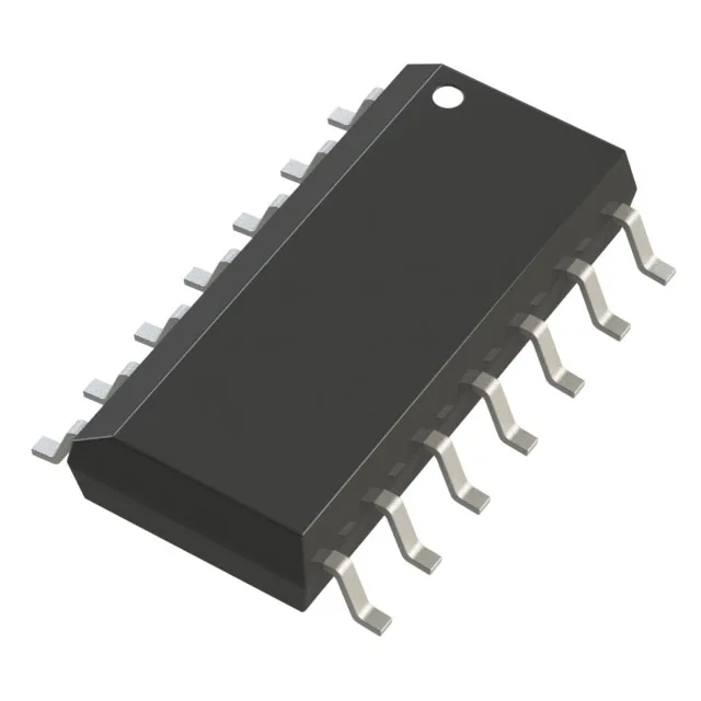
The part comes in a 14-SOIC package with a 3.90 mm body width (0.154"). Cut Tape quantities are also available for prototyping. Surface-mount only — no through-hole variant exists. The 14-SOIC footprint is standard, so existing land patterns for quad op-amps in this package work without modification.