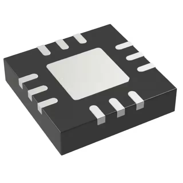
Single LVDS comparator with latch — 3 ns decision speed
The AD8465WBCPZ-WP is a single high-speed comparator from Analog Devices' Automotive series, featuring a latched output that holds the comparison result until a reset signal releases it — useful for capturing fast transients in a sampled-data system where the downstream logic needs a stable decision window. With a 3 ns maximum propagation delay, this part resolves input differences within nanoseconds, making it suitable for overcurrent detection, zero-crossing circuits, and high-frequency threshold monitoring in automotive or industrial control loops. The 100 µV of built-in hysteresis prevents output chatter when the input signal lingers near the comparator threshold — a common issue in noisy environments like motor-drive feedback or sensor interfaces with slow edge rates.
Supply, output, and thermal envelope
The output stage provides complementary LVDS signals with rail-to-rail capability, so it drives either a differential pair into an LVDS receiver or a single-ended CMOS load — the complementary outputs also simplify interfacing to CML or PECL logic families with external termination. Housed in a 12-lead LFCSP-WQ (3 mm x 3 mm) package with an exposed pad, the footprint suits dense PCB layouts while the pad provides a low thermal resistance path to the board's ground plane — critical for maintaining junction temperature below the 125°C limit when the comparator drives a 50 mA output load continuously.
Noise immunity and DC accuracy
The 50 dB CMRR and 60 dB PSRR mean that common-mode voltage shifts on the input or ripple on the supply rail are attenuated by a factor of roughly 300 to 1000 before they appear as an apparent offset at the comparator input — in a 12 V battery monitoring circuit with 100 mV of supply ripple, the ripple-induced error at the comparator is under 100 µV.
ROHS3 compliant per, with no RoHS exemptions that would require special handling for EU-market products. The part ships in tray packaging, which is the standard format for volume assembly but may require re-reeling for pick-and-place lines that feed from tape — confirm the feeder compatibility at your contract manufacturer before committing the BOM line.