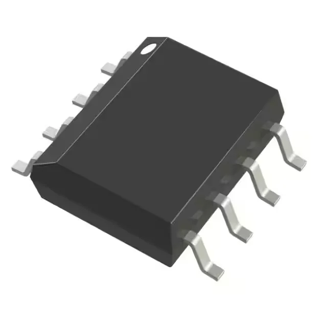
Analog Devices AD825ARZ — Memory (DRAM / SRAM / Flash / EEPROM)

AD825ARZ JFET Op-Amp, 140V/µs Slew Rate, 8-SOIC

MPNAD825ARZ
End of Life

Analog Devices AD825ARZ, JFET op-amp, single circuit, 140 V/µs slew rate, 46 MHz -3 dB bandwidth, 26 MHz gain bandwidth, 15 pA input bias, 1 mV offset, 6.5 mA supply, 8-SOIC package, -40°C to 85°C, Tube.

$5.96Ref. price · indicative, final on quote
Packaging8-SOIC (0.154", 3.90mm Width)
StockContact for availability
MOQ1 pcs
  • 100% new & originalTraceable channels only — no refurbs, no pulls, no remarked parts.
  • Date & lot codes on quoteStated per line before you commit; label photos on request.
  • MSL-compliant ESD packingMoisture-sealed bags with indicator cards; reels photo-verified.
  • PayPal buyer protectionPay by T/T, PayPal or Payoneer — card payments covered end to end.

Specifications

AD825ARZ Technical Specifications
ParameterValue
Mounting typeSurface Mount
Amplifier typeJ-FET
Voltage - input offset1 mV
Voltage - supply span36 V
Current - supply6.5mA
Current - input bias15 pA
Current - output (Channel)50 mA
Operating temperature-40°C ~ 85°C
-3db bandwidth46 MHz
Gain bandwidth product26 MHz
PackageTube
Slew rate140V/µs
Case8-SOIC (0.154\", 3.90mm Width)
Number of circuits1

Product details

JFET input: why the 15 pA bias current matters

The 15 pA input bias current is the hallmark of a JFET amplifier. In a photodiode transimpedance amplifier, that bias current adds directly to the signal — 15 pA is negligible compared to the nanoamp-level photocurrent, so the error stays below 1%. For a precision integrator, the bias current charges the feedback capacitor and creates a voltage ramp; at 15 pA, that drift is small enough to allow integration times of several seconds before the output drifts appreciably. The 1 mV input offset voltage is typical for a trimmed JFET stage; if the application demands sub-millivolt accuracy, a nulling circuit or chopper-stabilized alternative would be needed.

Package and supply — board-fit constraints

The AD825ARZ comes in an 8-SOIC package (0.154" body width, 3.90 mm). Supply voltage range is 10 V to 36 V total.

Sourcing and lifecycle — no LTB concern

The AD825ARZ carries an Active lifecycle status with ROHS3 compliance. It is sourced through independent distribution and quoted to order against an RFQ; availability and current pricing are confirmed at quote time.

Frequently asked questions

Does AD825ARZ come in tape and reel packaging?

The listed packaging for the AD825ARZ is Tube. If you need tape and reel, check the AD825ARZ-REEL7 variant or contact us with your volume — we can confirm alternate packaging options at quote time.

Is AD825ARZ RoHS compliant?

Yes, the AD825ARZ is ROHS3 compliant, meeting the latest EU RoHS directive requirements.

What is the pinout of AD825ARZ?

The AD825ARZ uses the standard 8-SOIC pinout for a single op-amp: pin 1 is offset null, pin 2 is inverting input, pin 3 is non-inverting input, pin 4 is V-, pin 5 is offset null, pin 6 is output, pin 7 is V+, pin 8 is NC. This matches the industry-standard SOIC-8 op-amp footprint.

Is AD825ARZ a direct replacement for AD845?

The AD845 is a different device with its own specifications. The AD825ARZ is a JFET input op-amp with 140 V/µs slew rate and 46 MHz bandwidth, while the AD845 is a bipolar input device. They are not direct pin-for-pin replacements; verify the circuit requirements before substituting.

What is the closest functional second-source to AD825ARZ?

The AD843JRZ-16 is a peer JFET op-amp with a 250 V/µs slew rate and 34 MHz bandwidth, but it has a commercial temperature range (0°C to 70°C) versus the AD825ARZ's industrial range (-40°C to 85°C). The AD8620ARZ-REEL7 is a dual JFET op-amp with 60 V/µs slew rate and wider temperature range (-40°C to 125°C). Neither is a drop-in replacement; evaluate the specific speed, temperature, and channel count needed.