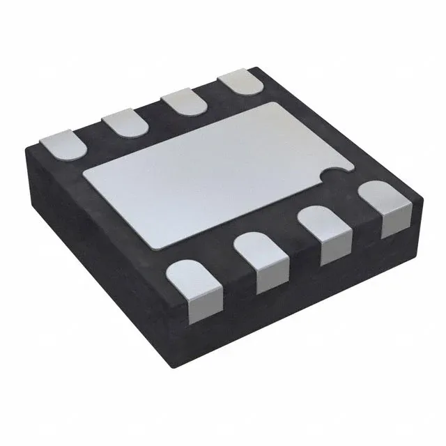
High-speed differential amplifier for ADC driving and signal conditioning
Its 410 MHz -3 dB bandwidth and 800 V/µs slew rate support wideband applications such as communications receivers, test instrumentation, and medical imaging front-ends. Operating from a single 4.5 V to 12 V supply or split supplies, it fits into 5 V and ±5 V systems without extra regulation. The 8-LFCSP (3x3) package with exposed pad provides a compact footprint and thermal path for dense layouts.
The 410 MHz -3 dB bandwidth ensures the amplifier maintains flat gain up to several hundred megahertz, critical for preserving the harmonic content of high-speed signals like those from a 14-bit, 250 MSPS ADC. Together, these specs keep the amplifier from becoming the bottleneck in a high-dynamic-range receiver or a wideband data-acquisition channel.
With a supply span from 4.5 V to 12 V, the AD8139ACPZ-R2 can be powered from a single 5 V rail (common in many ADC driver circuits) or from ±5 V supplies for bipolar signal handling. The 100 mA output current per channel provides enough drive to charge the sampling capacitor of a high-speed ADC or to drive a 50 Ω terminated line. The 24.5 mA supply current is a reasonable quiescent draw for this performance class — budget the thermal dissipation in the 3 mm × 3 mm LFCSP if the ambient runs near 125°C.
The wide temperature range also covers outdoor telecom cabinets and engine-bay electronics. The 150 µV input offset voltage and 2.25 µA input bias current are stable across temperature, so DC accuracy is maintained in precision measurement paths.
It is ROHS3 compliant. For new designs, this part can be qualified without planning for a last-time buy.