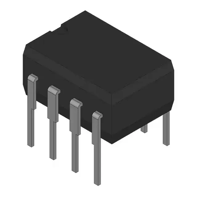
JFET op amp for military-temperature analog conditioning
The AD745SQ: It delivers a 20 MHz gain-bandwidth product and a 12V/µs slew rate, drawing 8 mA quiescent supply current.
The 12V/µs slew rate and 20 MHz -3 dB bandwidth are matched for fast pulse and wideband analog signals. A 10 V peak-to-peak output step slews in under 1 µs, which covers most sensor front-end and ADC driver requirements up to a few MHz. The 40 mA output current per channel gives enough drive for a 50 Ω line or a moderate capacitive load without external buffer stages.
Package and supply — design-in notes
Supply span runs from 9.6 V minimum to 36 V maximum, so it works on ±5 V, ±12 V, or ±15 V rails. The ceramic package is MSL 1 and withstands standard wave-solder profiles, but the RoHS non-compliant status means the leads are tin-lead plated — verify your assembly line's exemption or waiver before committing to a lead-free process.
The RoHS non-compliant designation is a sourcing flag for assemblies that require full RoHS exemption documentation, not a production-availability barrier.