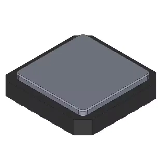
Analog Devices AD647SE — Analog & Data Acquisition

AD647SE JFET Op-Amp, Dual, 3 V/µs, 50 kHz, 20-CLCC

MPNAD647SE
End of Life

Analog Devices AD647SE, dual JFET operational amplifier, 3 V/µs slew rate, 50 kHz -3 dB bandwidth, 10 pA input bias, 500 µV offset, 10 V to 30 V supply, -55°C to 125°C, 20-CLCC ceramic package, Bulk.

$68.82Ref. price · indicative, final on quote
Packaging20-CLCC
RoHSRoHS non-compliant
Independent supplier — new & surplus stockAuthenticity-screened · ESD-safe packingListing updated Aug 2026

Specifications

AD647SE specifications
ParameterValue
MountingSurface Mount
Amplifier typeJ-FET
Voltage - input offset500 µV
Voltage - supply span30 V
Current - input bias10 pA
Current - output (Channel)25 mA
Operating temperature-55°C ~ 125°C
-3db bandwidth50 kHz
PackageBulk
Slew rate3V/µs
Case20-CLCC
Number of circuits2

Product details

Dual JFET op-amp in a hermetic 20-CLCC — built for the temperature extremes

The AD647SE is a dual JFET-input operational amplifier from Analog Devices, packaged in a 20-lead ceramic leadless chip carrier (20-CLCC).

Slew rate is 3 V/µs and -3 dB bandwidth is 50 kHz. Input bias current is 10 pA and input offset voltage is 500 µV.

Supply span is 10 V minimum to 30 V maximum. Package is 20-CLCC (9x9 mm).

Active lifecycle, RoHS non-compliant — plan accordingly

RoHS non-compliant per the lifecycle record.

Frequently asked questions

What is the AD647SE replacement?

There is no direct pin-compatible drop-in replacement for the AD647SE in the same 20-CLCC package. For a functional alternative with similar JFET performance in a plastic package, consider the ADA4062-4ARUZ (quad, 1.4 MHz, 3.3 V/µs, -40°C to 125°C, TSSOP) — but verify the supply voltage, temperature range, and pinout against your design.