JFET op-amp for precision analog in harsh environments
Its 10 pA input bias current and 1 mV offset voltage suit high-impedance sensor conditioning — photodiodes, pH probes, piezoelectric transducers — where bias current errors would otherwise swamp the signal. Supply flexibility spans 10 V to 36 V total, accommodating ±5 V to ±18 V dual rails or a single 12 V/24 V industrial bus.
The 13 V/µs slew rate defines the maximum rate of change at the output before slew-induced distortion sets in. For a 10 V peak-to-peak output swing, the full-power bandwidth works out to roughly 200 kHz — above that, the output waveform rounds off. In practice, keep signal frequencies well below the 50 kHz -3 dB bandwidth to stay inside the linear region. This is a deliberate trade-off: the JFET input stage delivers the low bias current and wide supply range, not video-speed settling.
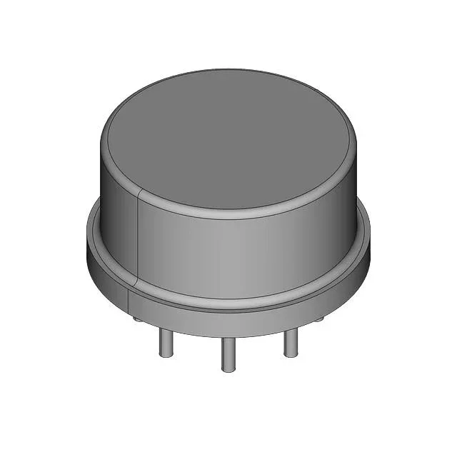
Hermetic TO-99-8 — package choice for mission-critical reliability
The TO-99-8 metal can is a hermetic package, sealed against moisture and contaminants. It is the standard choice for avionics, satellite, and downhole instrumentation where a plastic SOIC or DIP would risk corrosion or outgassing over a 20-year service life. The eight-pin circular footprint is through-hole only — no surface-mount variant exists for this part. Plan for hand-insertion or wave-solder assembly; the metal case also provides a degree of RF shielding, though it is not specified as such.
Note that it is RoHS non-compliant — the tin-lead finish is intentional for high-reliability solder joints in military and aerospace assemblies that are exempt from RoHS restrictions.