JFET input stage — what the 10 pA bias buys you
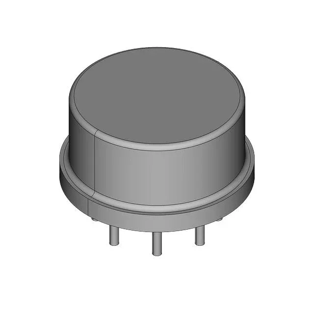
The AD542SH is a single-channel JFET-input operational amplifier from Analog Devices, housed in a hermetic TO-99-8 metal can. Supply span runs from 10 V to 36 V, giving ±5 V to ±18 V dual-supply flexibility, and the output can deliver 25 mA per channel. The 1 mV input offset voltage is adequate for general-purpose precision work, though a chopper-stabilized part would be needed for sub-100 µV applications.
TO-99-8 can — legacy footprint, hermetic seal
The TO-99-8 metal can is a through-hole package with a circular 8-pin layout on a 0.230-inch diameter base. It offers a hermetic seal, which matters in high-humidity or condensing environments where plastic SOIC packages can absorb moisture and shift offset over time. The metal can also provides some RF shielding, though at 50 kHz bandwidth that is rarely the driver. Layout follows the standard TO-99 pinout: offset null, inverting input, non-inverting input, V–, offset null, output, V+, and NC. The through-hole mounting means the part is not a candidate for high-density SMT boards, but it is straightforward to hand-assemble or retrofit into existing through-hole PCB designs.
If your BOM calls for an extended-temperature JFET op-amp, the AD542SH is the wrong pick — look for the industrial-grade AD542KH or similar.
For RoHS-compliant builds, a surface-mount JFET op-amp in an SOIC package (e.g., AD711JRZ) is the usual migration path.