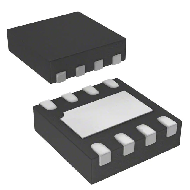
Renesas Electronics SLG55596AV — DC-DC Power Modules

SLG55596AV USB Data Switch, 1 GHz Bandwidth, 7 Ohm Rds(on)

MPNSLG55596AV
End of Life

Dialog Semiconductor SLG55596AV USB data switch, 2-channel, 1 GHz -3dB bandwidth, 7 Ohm max on-resistance, 4.5V to 5.5V supply, -40°C to 85°C, 8-TDFN (2x2) package.

$0.93Ref. price · indicative, final on quote
Packaging8-WFDFN Exposed Pad
StockContact for availability
MOQ1 pcs
  • 100% new & originalTraceable channels only — no refurbs, no pulls, no remarked parts.
  • Date & lot codes on quoteStated per line before you commit; label photos on request.
  • MSL-compliant ESD packingMoisture-sealed bags with indicator cards; reels photo-verified.
  • PayPal buyer protectionPay by T/T, PayPal or Payoneer — card payments covered end to end.

Specifications

SLG55596AV Technical Specifications
ParameterValue
Mounting typeSurface Mount
Voltage - supply, single (V+)4.5V ~ 5.5V
Operating temperature-40°C ~ 85°C (TA)
-3db bandwidth1GHz
PackageTape & Reel (TR); Cut Tape (CT)
ApplicationsUSB
Case8-WFDFN Exposed Pad
Number of channels2
On-State resistance7Ohm

Product details

1 GHz bandwidth — what it means for the USB bus

The SLG55596AV is a Dialog Semiconductor 2-channel analog switch designed for USB signal routing, with a -3dB bandwidth of 1 GHz. That bandwidth comfortably passes USB 2.0 High-Speed (480 Mbps) signals with minimal eye-diagram closure, and it also covers USB 1.1 Full-Speed (12 Mbps) without a second thought. The 7 Ohm max on-resistance keeps the DC voltage drop across the switch under 35 mV at the USB 2.0 signalling current, so the downstream device still sees a valid VBUS level. The part operates from a single 4.5V to 5.5V supply, matching the 5V USB VBUS rail directly, and it is specified over the -40°C to 85°C industrial temperature range — useful for USB ports on outdoor kiosks, factory-floor HMI panels, or any equipment that lives outside the climate-controlled office.

Package and footprint — 8-TDFN with exposed pad

The SLG55596AV comes in an 8-WFDFN exposed-pad package, supplier device package 8-TDFN (2x2 mm). The exposed pad is the main thermal path and also the ground connection — the PCB layout needs a via-in-pad or a thermal via array under the pad to keep the junction temperature within limits when switching the full 500 mA USB current. The 2x2 mm footprint is compact enough for space-constrained designs like USB-C dongles or portable docking stations. Surface-mount assembly is standard; no special reflow profile beyond the usual lead-free soak.

Lifecycle and sourcing reality

The SLG55596AV carries an Active product status and is RoHS Compliant. For BOM planning, this means no imminent obsolescence risk for new designs.

Frequently asked questions

What is the on-resistance of the SLG55596AV?

The maximum on-state resistance is 7 Ohms, which keeps the voltage drop low for USB signalling.