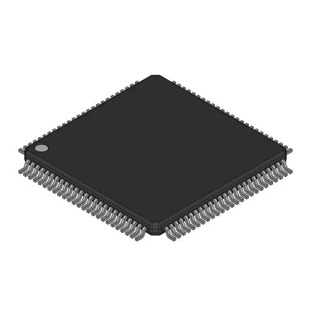
9 Mbit synchronous SRAM at 133 MHz — the 36-bit word width
The 71V67603ZS133PF is a 9 Mbit synchronous SRAM from Renesas, organized 256K x 36. The 36-bit word width maps directly to a 32-bit data bus with four parity or ECC bits — one chip covers the full bus plus error detection overhead that would otherwise require a separate 8-bit SRAM. Rated for a 133 MHz clock with a 4.2 ns access time. The access time is the pipeline latency from address latch to data-out; once the pipeline is filled, the part sustains back-to-back reads at the full 133 MHz rate. The 4.2 ns figure sets the timing budget for the FPGA or ASIC memory controller — the input setup and hold windows must close inside that window.
100-TQFP footprint and board integration
Packaged in a 100-lead LQFP (also designated 100-TQFP) with a 14 x 14 mm body and 0.5 mm pitch. The 0.5 mm pitch demands a 4-layer PCB for clean fan-out — two-layer boards can only route the outer rows, leaving the inner power and ground balls unconnected. This limits the part to indoor, climate-controlled environments — no extended-temp or industrial variants are specified on this order code.
Active lifecycle, RoHS non-compliant — the sourcing read
RoHS non-compliant. This is the legacy tin-lead finish, not the Pb-free version. If the BOM requires RoHS exemption 7(c)-I (lead in high-melt-temperature solder) or a customer waiver, this part qualifies; if the assembly line is RoHS-only with no Pb exemption, order the Pb-free suffix variant instead. The non-compliant status is a hard gate for some EMS houses — confirm the solder profile before committing the line item.