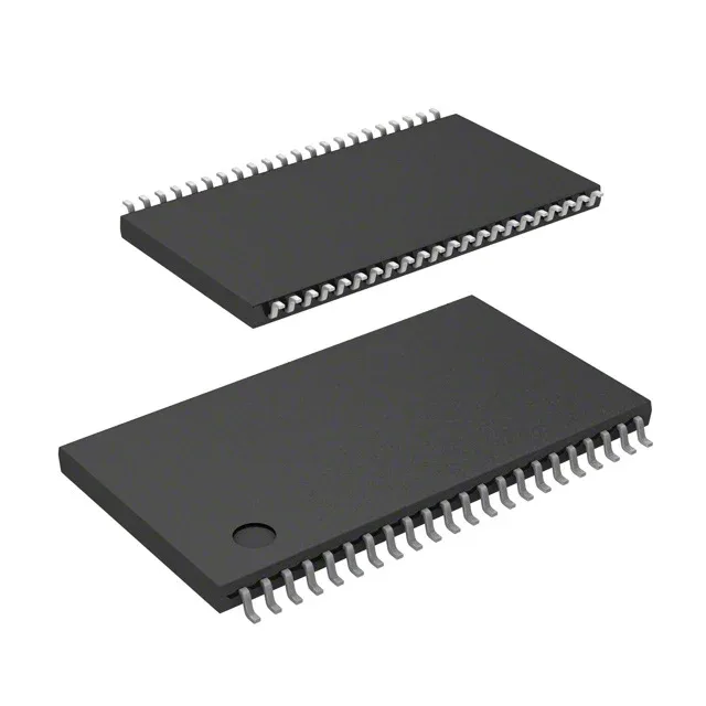
Renesas Electronics 71V424S10PHG — Analog & Data Acquisition

Renesas 71V424S10PHG SRAM, 4Mbit, 10ns, 44-TSOP II

MPN71V424S10PHG
End of Life

Renesas Electronics 71V424S10PHG asynchronous SRAM, 4Mbit, 512K x 8 organization, 10 ns access time, 3V to 3.6V supply, 44-TSOP II, tube.

$8.79Ref. price · indicative, final on quote
Packaging44-TSOP (0.400", 10.16mm Width)
StockContact for availability
Lead timeIn Stock wk
MOQ1 pcs
  • 100% new & originalTraceable channels only — no refurbs, no pulls, no remarked parts.
  • Date & lot codes on quoteStated per line before you commit; label photos on request.
  • MSL-compliant ESD packingMoisture-sealed bags with indicator cards; reels photo-verified.
  • PayPal buyer protectionPay by T/T, PayPal or Payoneer — card payments covered end to end.

Specifications

71V424S10PHG Technical Specifications
ParameterValue
Memory typeVolatile
Mounting typeSurface Mount
Voltage3V ~ 3.6V
Memory interfaceParallel
Operating temperature0°C ~ 70°C (TA)
PackageTube
TechnologySRAM - Asynchronous
Access time10 ns
Memory size4Mbit
Memory formatSRAM
Case44-TSOP (0.400\", 10.16mm Width)
Memory organization512K x 8
Write cycle time - word, page10ns

Product details

Package and board-fit — 44-TSOP II footprint

The 71V424S10PHG: This is the standard thin small-outline package for high-density SRAM — the 0.8 mm pin pitch and 44-lead count match the JEDEC MO-142 footprint, so the board layout follows a known land pattern without custom pad geometry. Surface-mount assembly with the 10 ns access time means the part keeps up with a 100 MHz bus without wait states, provided the PCB trace length from the memory controller to the TSOP is kept under 150 mm to hold the signal-integrity budget.

512K x 8 organization — the byte-wide bus decision

Organised as 512K words of 8 bits each, this SRAM presents a byte-wide parallel interface. For an 8-bit microcontroller or a 32-bit processor that can byte-lane address individual memory banks, the 512K x 8 map simplifies the address decoding — the upper address lines select the chip, and the lower 19 lines (A0–A18) cycle through the 512K locations. The 10 ns write cycle time (word, page) matches the read access, so the bus turnaround is symmetric — no extra idle cycles needed between read and write bursts when the controller's memory timing is set for 10 ns.

Frequently asked questions

What is the closest functional second-source to 71V424S10PHG?

The 71V416L10BEG is a 4 Mbit asynchronous SRAM with the same 10 ns access time, but organised as 256K x 16 rather than 512K x 8. The 71V416L10BEG comes in a tray package and uses a 3.0 V supply. The pinout differs — the 71V416L10BEG is a 44-pin TSOP but the data bus width is 16 bits, so a board designed for the 71V424S10PHG's byte-wide bus would need a layout change to accommodate the wider data path.

What compliance documentation does Renesas provide for 71V424S10PHG?

The part is RoHS3 compliant. Standard Renesas documentation includes a datasheet, RoHS certificate of compliance, and material declaration. No REACH, UL, or IEC certification is listed in the available records.