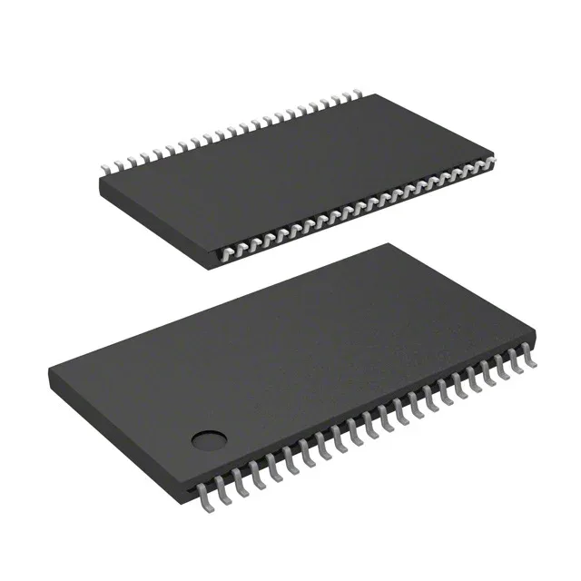
Renesas Electronics 71V416L15PHG — Analog & Data Acquisition

Renesas 71V416L15PHG 4Mbit Async SRAM, 15 ns, 44-TSOP II

MPN71V416L15PHG
End of Life

Renesas Electronics 71V416L15PHG asynchronous SRAM, 4 Mbit (256K x 16), 15 ns access time, parallel interface, 44-TSOP II, tray.

$8.79Ref. price · indicative, final on quote
Packaging44-TSOP (0.400", 10.16mm Width)
StockContact for availability
Lead timeIn Stock wk
MOQ1 pcs
  • 100% new & originalTraceable channels only — no refurbs, no pulls, no remarked parts.
  • Date & lot codes on quoteStated per line before you commit; label photos on request.
  • MSL-compliant ESD packingMoisture-sealed bags with indicator cards; reels photo-verified.
  • PayPal buyer protectionPay by T/T, PayPal or Payoneer — card payments covered end to end.

Specifications

71V416L15PHG Technical Specifications
ParameterValue
Memory typeVolatile
Mounting typeSurface Mount
Voltage3V ~ 3.6V
Memory interfaceParallel
Operating temperature0°C ~ 70°C (TA)
PackageTray
TechnologySRAM - Asynchronous
Access time15 ns
Memory size4Mbit
Memory formatSRAM
Case44-TSOP (0.400\", 10.16mm Width)
Memory organization256K x 16
Write cycle time - word, page15ns

Product details

Active lifecycle — no end-of-life risk on this BOM line

The 71V416L15PHG: For a procurement desk managing a 4 Mbit async SRAM line, this means the part stays in the manufacturer's active price book and allocation queue; there is no forced redesign window. ROHS3 compliant — no exemption expiry to track for EU/RoHS markets. The compliance documentation covers the full material declaration per JEDEC JESD97.

15 ns access time — the bus-speed ceiling for the memory controller

15 ns access time and 15 ns write cycle time set the minimum cycle period for the memory controller. At 15 ns the part supports a 66 MHz bus clock with zero wait states — the controller must meet the address-to-data valid window, not the other way around. For a 50 MHz bus there is margin; for a 75 MHz bus the controller needs a wait state insertion. The 256K x 16 organization maps directly onto a 16-bit data bus without byte-lane multiplexing — the chip-enable and output-enable signals gate the full word. This saves two GPIOs compared to a 32-bit-wide part in the same density class.

3V to 3.6V supply means a single 3.3V rail powers the core and I/O — no separate Vddq. 44-TSOP II package — the 0.400-inch body width, 10.16 mm, with 0.8 mm pin pitch. Standard footprint for 4 Mbit async SRAMs; rework-friendly with a hot-air nozzle sized for the 44-lead gull-wing profile.

Frequently asked questions

Will 71V416L15PHG drop into a board laid out for 71V416L10BEG?

Yes — both parts share the same 44-TSOP II footprint (0.400", 10.16 mm width) and the same 256K x 16 organization. The only parametric difference is the access time: 15 ns here versus 10 ns on the L10BEG.