Renesas Electronics 71V016SA20YGI — Microcontrollers & Processors (MCU / MPU / DSP)

Renesas 71V016SA20YGI SRAM, 1 Mbit, 20 ns, 44-SOJ

MPN71V016SA20YGI
End of Life

Renesas Electronics 71V016SA20YGI asynchronous SRAM, 1 Mbit (64K x 16), 20 ns access time, 3V-3.6V supply, -40°C to +85°C, 44-SOJ package, Bulk.

$2.49Ref. price · indicative, final on quote
Packaging44-BSOJ (0.400", 10.16mm Width)
StockIn Stock (16)
Lead timeIn Stock wk
MOQ1 pcs
  • 100% new & originalTraceable channels only — no refurbs, no pulls, no remarked parts.
  • Date & lot codes on quoteStated per line before you commit; label photos on request.
  • MSL-compliant ESD packingMoisture-sealed bags with indicator cards; reels photo-verified.
  • PayPal buyer protectionPay by T/T, PayPal or Payoneer — card payments covered end to end.

Specifications

71V016SA20YGI Technical Specifications
ParameterValue
Memory typeVolatile
Mounting typeSurface Mount
Voltage3V ~ 3.6V
Memory interfaceParallel
Operating temperature-40°C ~ 85°C (TA)
PackageBulk
TechnologySRAM - Asynchronous
Access time20 ns
Memory size1Mbit
Memory formatSRAM
Case44-BSOJ (0.400\", 10.16mm Width)
Memory organization64K x 16
Write cycle time - word, page20ns

Product details

Active production, 20 ns asynchronous SRAM for 3.3V buses

The Renesas 71V016SA20YGI is a 1 Mbit asynchronous SRAM organised as 64K words by 16 bits, with a 20 ns access time that sets the bus-speed floor for the memory interface.

Board-fit: 44-SOJ package and industrial temperature range

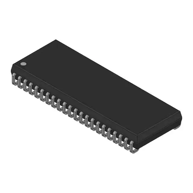
The 44-SOJ (Small Outline J-lead) package, 0.400-inch body width, is a surface-mount footprint with J-bend leads that self-align during reflow and give good visual solder-joint inspection access. Bulk packaging (tubes or trays) means the parts are not on tape-and-reel — factor that into your pick-and-place feeder setup if the line expects reeled components.

Memory interface: parallel, no clock, simple strobe timing

Asynchronous SRAM needs no clock — the address is latched by chip-enable and write-enable strobes, so the timing closure on the PCB is just propagation delay and setup/hold margins, not a clock-tree skew budget. Write cycle time matches the read access time at 20 ns, so the bus can switch between read and write at the same rate without wait states. The 64K x 16 organisation gives a 16-bit data bus in one chip — no need to pair two 8-bit-wide parts for a 16-bit system.

Frequently asked questions

What is the 71V016SA20YGI's access time and why does it matter?

The access time is 20 ns. For a 3.3V system running at 50 MHz (20 ns period), the SRAM's 20 ns access consumes the entire cycle — the controller must latch data at the end of the cycle without additional wait states.

What package does the 71V016SA20YGI use?

It comes in a 44-SOJ (Small Outline J-lead) package, 0.400-inch body width.