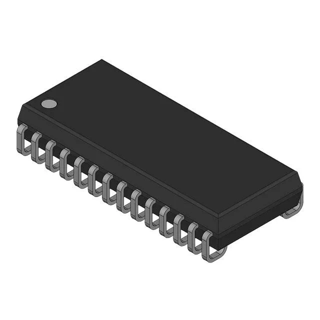
20 ns asynchronous SRAM for byte-wide memory maps
The 7164L20YG is a 64Kbit asynchronous SRAM organized as 8K x 8, with a 20 ns access time and a matching 20 ns write cycle. The 20 ns access time sets the read-cycle ceiling: the processor must assert the chip-enable and output-enable signals and wait at least 20 ns before the data bus is valid. For a 40 MHz bus clock (25 ns period), this leaves 5 ns of margin after address setup — tight but workable with proper board timing.
28-SOJ footprint and board integration
The J-lead form factor provides a smaller board footprint than a DIP while maintaining through-hole-like solder-joint inspection access. The surface-mount package (Mounting Type: Surface Mount) suits automated pick-and-place assembly. The 28-SOJ is a common pinout for 8K x 8 SRAMs — many 64Kbit parts from other vendors share the same footprint, easing second-sourcing if the BOM needs a backup.