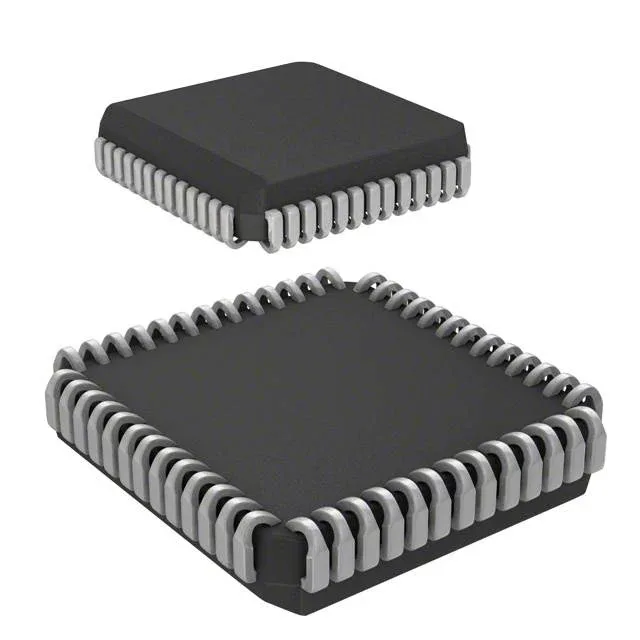
Dual-port asynchronous SRAM in a 52-PLCC — what you get
The Renesas 71321SA55JG8 is a 16Kbit (2K x 8) dual-port asynchronous SRAM. Unlike a single-port memory, the dual-port architecture gives two independent controllers simultaneous read/write access to the same memory array through separate address, data, and control buses. The 55 ns access time and 55 ns write cycle time are matched, so the bus timing is symmetric. At 5V nominal (4.5V–5.5V supply,) this part sits comfortably in legacy 5V systems — think industrial PLCs, telecom line cards, or older test equipment that still run on 5V logic and haven't migrated to 3.3V or 1.8V domains. The 52-PLCC package with J-leads is a surface-mount footprint that is noticeably larger than modern fine-pitch packages (19.13 mm square,), but it is straightforward to hand-solder and inspect under a microscope. That makes it a practical choice for low-volume production runs, prototype boards, or field-service rework where a BGA or QFN would be impractical.
55 ns access — timing margin on a 5V bus
At 55 ns, the access time is the slowest rating on this part and the one that decides whether it can interface with your controller without wait states. A 5V microcontroller running at 20 MHz has a 50 ns clock period — this SRAM's 55 ns access means the controller will need at least one wait state for a read cycle. For a 10 MHz bus (100 ns period), the 55 ns access fits with 45 ns of margin, so zero-wait-state operation is possible. Check your controller's memory-cycle timing against the 55 ns access and 55 ns write cycle before committing the BOM line.
For a BOM that needs multi-year supply assurance, this part does not carry the obsolescence flag that some older dual-port SRAMs do. It is also RoHS3 compliant, which keeps it usable in new designs bound for EU or RoHS-regulated markets without an exemption.