256Kbit asynchronous SRAM for 5V bus systems
The Renesas 71256SA20PZG is a 256 Kbit asynchronous SRAM organized as 32K words by 8 bits. With a 20 ns access time and matching 20 ns write cycle, this part keeps up with fast 8-bit microcontrollers and DSPs that need zero-wait-state SRAM at clock rates up to 50 MHz.
Timing margin and bus interface
For a processor running at 50 MHz with a 20 ns cycle, this SRAM meets the setup time without an extra wait state — the address-to-data path fits within one clock period. As an asynchronous device, it needs no external clock — the chip enable and output enable pins gate the data bus directly. This simplifies the PCB layout because there is no clock trace to route and no PLL to lock.
Package and board integration
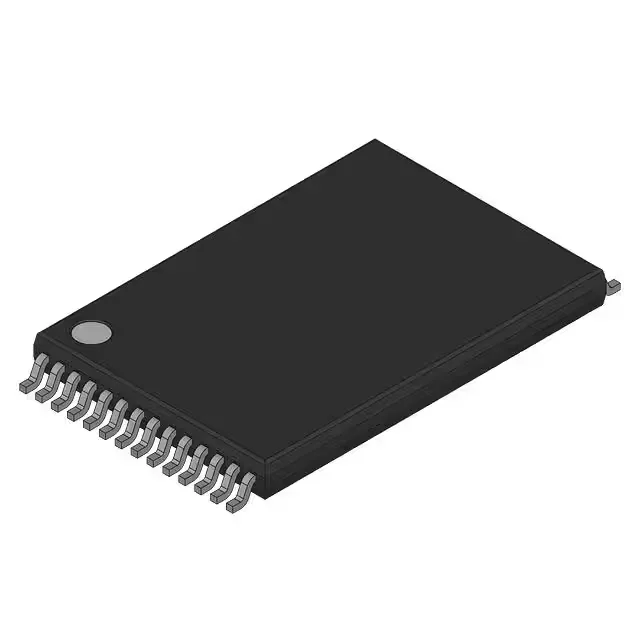
Housed in a 28-TSSOP package (0.465" body width, 11.80 mm), the part is surface-mount with a 0.65 mm pin pitch typical for this form factor. The 28-TSOP supplier device package is the same mechanical outline — the two names refer to the same footprint. Decoupling with a 0.1 µF ceramic capacitor close to each VDD pin is standard practice for this access time.
Temperature grade and operating range
It is suited for office equipment, test instrumentation, and industrial control panels that stay within indoor climate — not for extended outdoor or under-hood automotive use. The memory is volatile — data is retained only while power is applied. For non-volatile storage in the same socket, a battery-backed SRAM module or an FRAM would be the alternative, but that changes the pinout and supply requirements.
Sourcing and lifecycle status
Supplied in Bulk packaging — not tape-and-reel — which means the parts ship in tubes or trays. For automated pick-and-place, a tube-to-reel transfer or a separate tape-and-reel order variant may be needed if the line is set up for reel feed.