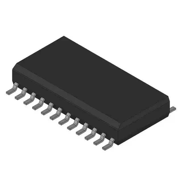
35 ns access, 2K × 8, 5 V — the JEDEC 24-SOIC footprint
The 6116LA35SO is a 16 Kbit asynchronous SRAM organized 2K × 8, with a 35 ns access time and a matching 35 ns write cycle. The parallel interface — 11 address lines, 8 data I/O, plus chip enable, output enable, and write enable — follows the JEDEC 24-pin SRAM pinout. A board laid out for an Alliance Memory AS6C1008 or ISSI IS61C256A in the same 24-SOIC footprint accepts this part without a layout change.
Commercial temp, 5 V only — screening for the application
A design that must operate at -40 °C or +85 °C ambient requires the industrial-temperature suffix (6116LA35SOI or similar). RoHS non-compliant. The lead finish or die-attach material contains lead, which is typical for high-reliability or legacy SRAM products. This part qualifies under EU RoHS exemption 7c-I for applications where lead in solder is still permitted (aerospace, medical, certain industrial controls). For a RoHS-compliant BOM, the lead-free equivalent (6116LA35SO-T or similar) must be verified against the same timing and package.
Active production — no end-of-life watch
The 24-SOIC footprint is shared by multiple vendors (Alliance, ISSI, Cypress), so a second-source cross-reference can be evaluated at RFQ time if single-source risk is a concern.