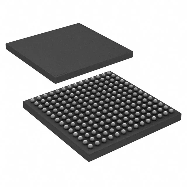
The MIMXRT1051DVJ6B runs the ARM Cortex-M7 core at 600 MHz, which puts it in the crossover MCU class — compute performance that rivals low-end application processors, but with the deterministic interrupt latency and real-time control of an MCU. That 600 MHz clock is the headline number; it drives the part's ability to run graphics stacks, Ethernet TCP/IP offload, and DSP-style audio processing without an external MPU.
External program memory — BOM planning note
This device has no on-chip Flash for program storage. Code executes from external memory — typically a SPI NOR flash or a parallel NAND via the EBI/EMI interface. The 512K×8 internal RAM serves as tightly coupled or general-purpose data memory. Designers need to budget for an external memory device and account for the boot sequence: the internal ROM loader supports serial download from SPI, SDIO, or USB before jumping to the external image.
Rated for 0°C to 95°C junction temperature. Suitable for conditioned indoor environments.
Connectivity and I/O
127 GPIOs and a connectivity set that includes Ethernet, CANbus, USB OTG, SDIO, SAI, and SPDIF make this part a natural fit for a board that needs to bridge fieldbus traffic to an Ethernet backbone, or drive a local display while logging data to an SD card. The 20-channel 12-bit ADC is there for analog sensing — panel potentiometers, current shunts, thermistor inputs — but the real ENOB at 600 MHz system clock depends on the ADC sample rate and the analog front-end noise floor.
Package and supply
196-ball LFBGA, 12×12 mm body. Surface-mount only. Supply range is 3V to 3.6V.
NXP lists the MIMXRT1051DVJ6B as Active.