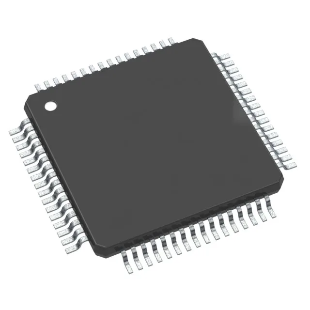
The NXP LPC5534JBD64E is a 32-bit ARM Cortex-M33 single-core MCU running at 150 MHz, with 128 KB Flash and 96 KB RAM. It targets real-time control and mixed-signal acquisition in industrial and automotive-adjacent environments, with a -40°C to 105°C operating range and a 1.8 V to 3.6 V supply. The Flexcomm engine lets each serial interface be configured as I²C, SPI, UART, I²S, or I³C without adding external muxing — a practical BOM shrink for boards that need to talk to a sensor hub on I²C and a display on SPI from the same pin block.
128 KB Flash, 96 KB RAM — sizing the firmware budget
The 128 KB Flash and 96 KB RAM support a modest RTOS and CANopen stack.
Flexcomm and CANbus — wiring the serial backbone
Flexcomm is the headline peripheral: each of the serial blocks can be assigned as I²C, SPI, UART, I²S, or I³C at runtime. That means a single board design can reuse the same pin assignment for a production variant that swaps an I²C temperature sensor for an SPI flash without a PCB spin. CANbus is present for industrial or automotive-adjacent networks; the 39 GPIO count provides enough headroom for a local I/O bank plus a parallel LCD or keypad matrix.
13×16-bit ADC and 1×12-bit DAC — analog front-end fit
Thirteen 16-bit ADC channels and a single 12-bit DAC cover typical multi-sensor acquisition and one analog output channel. The 16-bit resolution is suited for load-cell or thermocouple conditioning where 12-bit would leave noise on the table; the DAC handles set-point generation or analog trim. Both converters share the same supply rail, so keep the analog and digital grounds clean — the exposed pad on the 64-HTQFP helps with thermal and ground-plane coupling.
The LPC5534JBD64E has an Active lifecycle status.