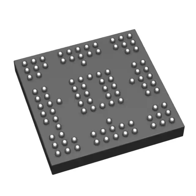
NXP USA Inc. LPC5526JEV98K — Microcontrollers & Processors (MCU / MPU / DSP)

NXP LPC5526JEV98K ARM Cortex-M33 MCU, 150 MHz, 256 KB Flash, 98-VFBGA

MPNLPC5526JEV98K
Active

NXP LPC552x series 32-bit ARM Cortex-M33 single-core MCU, 150 MHz, 256 KB Flash, 144 KB SRAM, 64 GPIO, USB and Flexcomm connectivity, 10-channel 16-bit ADC, 1.8 V–3.6 V supply, -40°C to 105°C, 98-VFBGA (7x7 mm), tray packaging.

$8.6100Ref. price · indicative, final on quote
Packaging98-VFBGA
RoHSROHS3 Compliant
SeriesLPC552x
Independent supplier — new & surplus stockAuthenticity-screened · ESD-safe packingListing updated Jul 2026

Specifications

LPC5526JEV98K specifications
ParameterValue
SeriesLPC552x
MountingSurface Mount
Oscillator typeInternal
Program memory typeFLASH
Voltage - supply (Vcc (Vdd))1.8V ~ 3.6V
Operating temperature-40°C~105°C(TA)
Speed150MHz
PackageTray
RAM size144K x 8
Core size32-Bit Single-Core
PeripheralsBrown-out Detect/Reset, DMA, I²S, POR, PWM, WDT
ConnectivityFlexcomm, I²C, MMC/SD/SDIO, SPI, UART/USART, USB
Number of i (O)64
Core processorARM® Cortex®-M33
Case98-VFBGA
Data convertersA/D 10x16b
Program memory size256KB (256K x 8)

Product details

The NXP LPC5526JEV98K is a 32-bit ARM Cortex-M33 single-core MCU clocked at 150 MHz with 256 KB Flash and 144 KB SRAM. It packs 64 GPIO, USB, Flexcomm serial interfaces, and a 10-channel 16-bit ADC into a 98-VFBGA (7x7 mm) package. The 1.8 V to 3.6 V supply range and -40°C to 105°C operating temperature qualify it for industrial control, sensor fusion, and connected edge nodes where a compact BGA footprint and wide thermal margin are required.

150 MHz Cortex-M33 — what that means for throughput

The 150 MHz clock on the ARM Cortex-M33 core delivers integer DSP and single-cycle multiply-accumulate (MAC) operations, plus the TrustZone security extension for isolated execution domains. That clock rate positions this MCU for real-time control loops, audio processing, and protocol bridging where the CPU must service USB, I²C, SPI, and UART traffic without stalling the application thread.

144 KB SRAM — buffer headroom for connectivity stacks

144 KB of on-chip SRAM (organized as 144K x 8) supports multi-packet USB buffers, audio sample queues, and dual-protocol stacks without external memory. That is enough for a USB CDC-ACM + I²C sensor hub or a small RTOS with several tasks; designs needing larger frame buffers (e.g., camera pipelines) will want the LPC55S6x variant with additional SRAM.

No end-of-life notice is published.

Frequently asked questions

Where can I find the LPC5526JEV98K datasheet?

The LPC5526JEV98K datasheet is published by NXP and covers the full LPC552x series, including electrical characteristics, memory map, peripheral register descriptions, and package drawing for the 98-VFBGA.

Is LPC5526JEV98K suitable for -40°C to 105°C applications?

Yes, the LPC5526JEV98K is rated for -40°C to 105°C operating temperature, making it suitable for industrial, automotive cabin, and outdoor equipment that must function across a wide thermal range.

How does LPC5526JEV98K compare to the LPC5526JEV98?

The LPC5526JEV98 is a functional cross-reference to the LPC5526JEV98K, sharing the same Cortex-M33 core, memory, and peripheral set. Verify package compatibility — the JEV98 variant may use a different package code; confirm the footprint matches your layout before substituting.