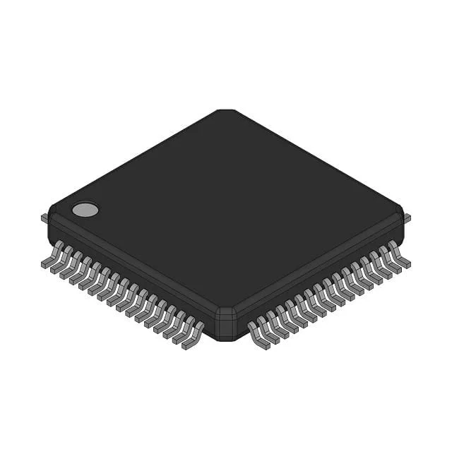
NXP USA Inc. LPC54102J512BD64151 — Microcontrollers & Processors (MCU / MPU / DSP)

NXP LPC54102J512BD64151 32-bit Dual-Core MCU, 100MHz

MPNLPC54102J512BD64151
Active

NXP LPC54100 series, LPC54102J512BD64151, 32-bit dual-core ARM Cortex-M4/M0+ at 100MHz, 512KB Flash, 104KB RAM, 50 I/O, 12x 12-bit ADC, I²C/SPI/UART, 1.62–3.6V, -40°C to 105°C, 64-LQFP (10x10mm), surface mount.

$12.0000Ref. price · indicative, final on quote
Independent supplier — new & surplus stockAuthenticity-screened · ESD-safe packingListing updated Jul 2026

Specifications

LPC54102J512BD64151 specifications
ParameterValue
SeriesLPC54100
MountingSurface Mount
Oscillator typeInternal
Program memory typeFLASH
Voltage - supply (Vcc (Vdd))1.62V ~ 3.6V
Operating temperature-40°C~105°C(TA)
Speed100MHz
PackageBulk
RAM size104K x 8
Core size32-Bit Dual-Core
PeripheralsBrown-out Detect/Reset, POR, PWM, WDT
ConnectivityI²C, SPI, UART/USART
Number of i (O)50
Core processorARM® Cortex®-M4/M0+
Case64-LQFP
Data convertersA/D 12x12b
Program memory size512KB (512K x 8)

Product details

Dual-core architecture — asymmetric processing without the power penalty

The NXP LPC54102J512BD64151 pairs a 100 MHz ARM Cortex-M4 with a Cortex-M0+ on the same die, splitting DSP-capable compute from background housekeeping. The M4 handles sensor fusion, audio processing, or control loops while the M0+ manages I²C/SPI/UART traffic, wake-up logic, and power-state transitions. This asymmetric dual-core approach lets the M4 sleep during light loads, drawing only the M0+ current, which keeps the active power profile lower than a single-core part at equivalent throughput.

Memory and I/O budget for BOM fit

512 KB Flash and 104 KB RAM support firmware with a real-time OS and sensor libraries. The 50 GPIOs and 12-channel 12-bit ADC cover mixed-signal interfaces without an external mux.

Frequently asked questions

Does LPC54102J512BD64151 have dual-core ARM Cortex-M4 and M0+?

Yes, it integrates a 100 MHz ARM Cortex-M4 and a Cortex-M0+ on a single die, enabling asymmetric processing where the M4 handles compute-intensive tasks and the M0+ manages I/O and power states.

What is the pinout of LPC54102J512BD64151?

The pinout follows the standard 64-LQFP (10x10 mm) assignment for the LPC54100 series. The supplier device package is 64-LQFP (10x10). For exact pin functions and alternate configurations, refer to the NXP LPC5410x user manual.

What is the difference between LPC54102 and LPC54114?

The LPC54114 is a higher-density variant with 256 KB Flash and 256 KB RAM, compared to the LPC54102's 512 KB Flash and 104 KB RAM. Both share the same 64-LQFP footprint, dual-core architecture, and peripheral set, making the LPC54114 a drop-in upgrade for designs requiring more RAM.