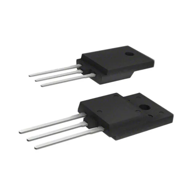
800 V, 11 A — the switching envelope for this CoolMOS N-channel
Conduction and switching — what the parametric ratings drive
The 450 mOhm Rds(on) at 10 V gate drive sets the I²R conduction loss at 11 A to about 54 W — the 34 W maximum power dissipation at the case (Tc) means the device must be heatsunk to stay within the SOA at full current. Input capacitance is 1600 pF at 100 V drain-source — this sets the switching energy stored in the Miller plateau and influences the turn-on delay.
Package and thermal — through-hole with an isolated tab
Through-hole mounting suits point-of-load and bulk-power stages where the PCB is not the primary thermal path.
The wide temperature envelope also covers outdoor telecom and factory-floor equipment.