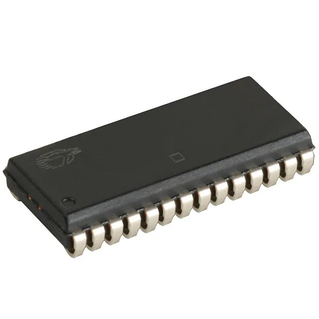
Infineon Technologies CY7C1399BNL-15VXC — Memory (DRAM / SRAM / Flash / EEPROM)

CY7C1399BNL-15VXC Cypress 256Kbit Async SRAM, 15ns, 3.3V, SOJ-28

MPNCY7C1399BNL-15VXC
Obsolete

Cypress CY7C1399BNL-15VXC; 256Kbit asynchronous SRAM; 15 ns access time; 3 V–3.6 V supply; 32K x 8 parallel organization; 28-BSOJ (0.300", 7.62 mm) surface-mount package; 0°C–70°C operating temperature. Tube packaging.

$1.6000Ref. price · indicative, final on quote
StockContact for availability
MOQ1 pcs
  • 100% new & originalTraceable channels only — no refurbs, no pulls, no remarked parts.
  • Date & lot codes on quoteStated per line before you commit; label photos on request.
  • MSL-compliant ESD packingMoisture-sealed bags with indicator cards; reels photo-verified.
  • PayPal buyer protectionPay by T/T, PayPal or Payoneer — card payments covered end to end.

Specifications

CY7C1399BNL-15VXC Technical Specifications
ParameterValue
Memory typeVolatile
Mounting typeSurface Mount
Voltage3V ~ 3.6V
Memory interfaceParallel
Operating temperature0°C ~ 70°C (TA)
PackageTube
TechnologySRAM - Asynchronous
Access time15 ns
Memory size256Kbit
Memory formatSRAM
Case28-BSOJ (0.300\", 7.62mm Width)
Memory organization32K x 8
Write cycle time - word, page15ns

Frequently asked questions

Is the CY7C1399BNL-15VXC obsolete?

Yes — the lifecycle stage is end-of-life hot under. Standard distribution is no longer active; sourcing is allocation recovery or broker channel only.

Does the 3 V–3.6 V supply handle brownout to 2.9 V?

No. The operating minimum is 3 V — a 2.9 V brownout during a motor-stall event falls outside the rated window and risks data corruption. The design needs a hold-up circuit or supply supervision if that event is a real-world case.

Is 15 ns access time compatible with a 50 MHz FPGA interface?

Yes. 50 MHz gives a 20 ns cycle; 15 ns access is well within that window. Write cycle time is also 15 ns symmetric, so a single firmware timing budget covers both read and write operations.