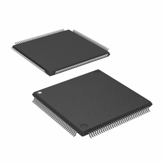
Infineon Technologies CY7C057V-12AXC — Memory (DRAM / SRAM / Flash / EEPROM)

CY7C057V-12AXC Infineon 1.152Mbit Dual-Port SRAM, 12ns

MPNCY7C057V-12AXC
Obsolete

Infineon Technologies CY7C057V-12AXC dual-port asynchronous SRAM, 1.152Mbit, 32K x 36 organization, 12 ns access time, 3V–3.6V supply, 144-LQFP tray, 0°C–70°C.

$139.9100Ref. price · indicative, final on quote
Independent supplier — new & surplus stockAuthenticity-screened · ESD-safe packingListing updated Jul 2026

Specifications

CY7C057V-12AXC specifications
ParameterValue
Memory typeVolatile
MountingSurface Mount
Voltage3V ~ 3.6V
Memory interfaceParallel
Operating temperature0°C~70°C(TA)
PackageTray
TechnologySRAM - Dual Port, Asynchronous
Access time12 ns
Memory size1.152Mbit
Memory formatSRAM
Case144-LQFP
Memory organization32K x 36
Write cycle time - word, page12ns

Product details

Infineon (formerly Cypress) lists the CY7C057V-12AXC as obsolete.

32K x 36 dual-port SRAM, 12 ns access

This is a 1.152 Mbit dual-port asynchronous SRAM organized as 32K words by 36 bits. The 12 ns access time and 12 ns write cycle time mean the part can complete a read or write operation in a single 83 MHz clock cycle — relevant for shared-memory designs where two controllers or processors need low-latency access to the same data buffer. The parallel memory interface connects directly to a standard SRAM bus without protocol overhead.

144-LQFP package — board-fit note

Supplied in a 144-lead LQFP tray, with the supplier device package specified as 144-TQFP (20x20). The 0.5 mm pitch LQFP footprint is a standard surface-mount package — the 20x20 mm body requires a reflow profile consistent with JEDEC MSL ratings typical for this class.

Frequently asked questions

What are the timing constraints for interfacing this SRAM to a 33 MHz bus or 50 ns wait-state microcontroller?

The 12 ns access time and 12 ns write cycle time are faster than a 33 MHz bus cycle (~30 ns), leaving comfortable margin for FPGA read-FSM timing closure. The 50 ns wait-state microcontroller bus easily satisfies the SRAM's write pulse width requirement. No byte-enable or bank-select details are available in the current evidence — confirm against the full Cypress datasheet for the 32K×36 word strobe architecture.