Clamping chain: standoff through breakdown to clamp
The 1.5SMCJ150 clamps at 268 V maximum under a 10/1000 µs surge waveform — that 268 V is the ceiling the downstream circuit never exceeds during a transients event. The reverse standoff sits at 150 V typical, meaning the diode stays invisible on the line under normal operation; it only transitions into avalanche breakdown above 167 V minimum. The window between 167 V and 268 V is where the clamping action lives — a 100 V headroom that absorbs the surge energy and shunts the excess current away from the protected rail.
The corresponding peak pulse current of 5.6 A is what the diode must survive for the duration of that pulse. Designing the board trace and bulk decoupling to survive a 5.6 A fault current for 20 ms is a different thermal problem than protecting against a nanosecond ESD event — the 1.5SMCJ150 is built for the slower, higher-energy surge, not the ultra-fast human-body model hit.
DO-214AB SMC package and surface-mount fit
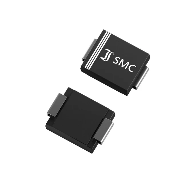
The SMC (DO-214AB) package is the standard medium-current TVS footprint — the cathode bar bridges the two mounting pads and acts as the primary thermal path to the board copper. Solder mask defined pads with a generous thermal land under the cathode tab carry the heat away during the clamping event; under-sizing the copper pour under the tab is the most common reason a TVS fails earlier than the datasheet predicts. The strip packaging option means it arrives on a reel or cut tape ready for standard SMT placement.
Junction temperature and thermal derating
The maximum junction temperature rating of 150 °C sets the upper bound of the thermal SOA — the part must stay below that TJ under continuous clamping duty or during a surge event.