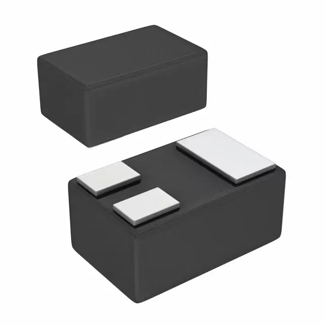
AEC-Q101 Zener TVS for automotive signal-line protection
The D5V0F2U3LPQ-7B: The 0.5 pF typical capacitance at 1 MHz keeps signal edges clean on high-speed interfaces such as CAN FD, LIN, or USB 2.0 — the low loading prevents eye-diagram closure that a higher-capacitance TVS would cause on a 12 Mbps or 480 Mbps bus. The X1-DFN1006-3 package (1.0 x 0.6 mm footprint) fits into dense I/O banks on multilayer automotive PCBs where board real estate is at a premium.
Clamp voltage and pulse current — the protection window
With a 5.5 V maximum standoff voltage, the device remains transparent below the signal rail and begins conducting when the line exceeds that threshold. The 6 V minimum breakdown voltage ensures the TVS does not clip a 5 V nominal supply during normal operation, even with a 10 % tolerance on the rail. For a 3.3 V CMOS input with a 5 V absolute-max rating, the 12 V clamp is within the typical margin for IEC 61000-4-2 level 4 (8 kV contact) transients, provided the series resistance on the board limits the current to the rated 1.5 A. The 1.5 A peak pulse current rating at the 8/20 µs waveform corresponds to an IEC 61000-4-5 surge level 1 or level 2 stress, depending on the source impedance. For a 50 Ω coupled surge, the 1.5 A translates to a 75 V open-circuit voltage — adequate for secondary protection after a bulk capacitor or a higher-energy TVS at the board input.
Active lifecycle and automotive compliance
It is suitable for new design-ins and ongoing production builds without a last-time-buy risk. AEC-Q101 qualification means the part has passed the full suite of automotive stress tests: high-temperature reverse bias (HTRB), temperature cycling, moisture sensitivity level (MSL) preconditioning, and ESD human-body-model (HBM) robustness per the AEC-Q101 rev-E standard. This is the minimum entry requirement for a tier-one ECU bill of material. The base product number D5V0F2 identifies the family; the -7B suffix denotes the tape-and-reel packaging option.