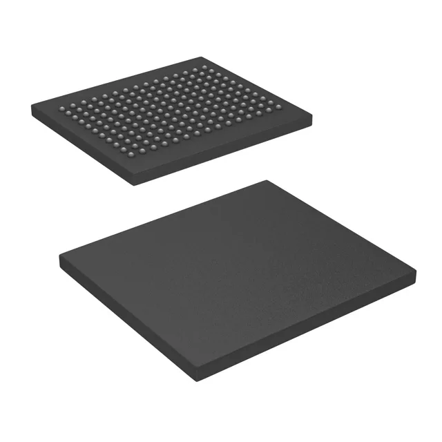
The Infineon CY7C1645KV18-450BZXI is a 144Mbit synchronous SRAM built on the QDR II+ architecture, clocked at 450 MHz with a 4M x 36 memory organization. QDR II+ eliminates the bus-turnaround dead cycles that plague conventional SRAM when switching between reads and writes — the data bus stays at full utilization on back-to-back transactions. The 36-bit wide data bus pairs naturally with a 36-bit FPGA or ASIC I/O bank running at 1.7 V to 1.9 V supply range. Typical deployment is in high-bandwidth packet buffers for network switches, base station line cards, or test equipment where deterministic latency and sustained throughput are non-negotiable.
Package and footprint — 165-FBGA (15x17 mm)
Supplied in a 165-ball FBGA, body size 15x17 mm. Surface-mount only. The ball map is specific to the 144Mbit x36 QDR II+ die; a 72Mbit x18 part like the CY7C1543KV18-400BZI uses a different FBGA footprint and will not align on the same PCB land pattern. Verify the layout against the Infineon package drawing before committing the board — the 15x17 mm form factor is not universal across the density range.