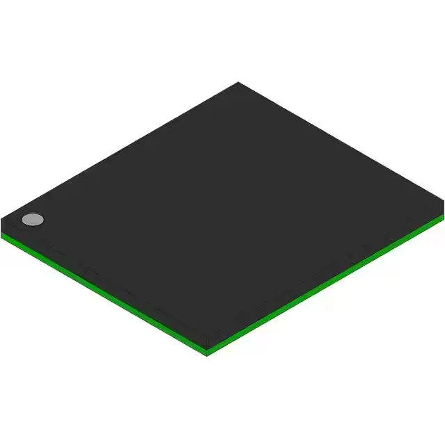
Cypress Semiconductor Corp CY7C1620KV18-300BZC — Memory (DRAM / SRAM / Flash / EEPROM)

Cypress CY7C1620KV18-300BZC 144Mbit DDR II SRAM, 300 MHz

MPNCY7C1620KV18-300BZC
Active

Cypress (Infineon) CY7C1620KV18-300BZC, 144 Mbit synchronous DDR II SRAM, 4M x 36 organization, 300 MHz clock, 1.7–1.9 V supply, 165-FBGA (15x17), 0°C to 70°C.

$215.4000Ref. price · indicative, final on quote
Independent supplier — new & surplus stockAuthenticity-screened · ESD-safe packingListing updated Jul 2026

Specifications

CY7C1620KV18-300BZC specifications
ParameterValue
Memory typeVolatile
MountingSurface Mount
Supply voltage1.7V ~ 1.9V
Clock frequency300 MHz
Memory interfaceParallel
Operating temperature0°C~70°C(TA)
PackageBulk
TechnologySRAM - Synchronous, DDR II
Memory size144Mbit
Memory formatSRAM
Case165-LBGA
Memory organization4M x 36

Product details

144 Mbit DDR II SRAM for high-throughput buffer applications

The Cypress (now Infineon) CY7C1620KV18-300BZC is a 144 Mbit synchronous DDR II SRAM organized as 4M by 36 bits. It clocks at 300 MHz on a parallel interface, delivering back-to-back read-write throughput without the dead cycles of a standard asynchronous SRAM. The 1.7 V to 1.9 V core supply and 165-FBGA (15x17) package target high-speed FPGA companion memory, network packet buffers, and DSP data caches where bus width and zero-bus-turnaround matter more than density.

At 300 MHz the DDR II interface transfers data on both clock edges. The 4M x 36 organization keeps the bus 36 bits wide.

Frequently asked questions

Will CY7C1620KV18-300BZC drop into a board designed for CY7C1650KV18-450BZC?

Both parts share the same 165-FBGA (15x17) package and 4M x 36 organization, so the footprint is identical. The 300 MHz part runs slower than the 450 MHz variant, so the board's timing closure at 300 MHz must be verified — the PCB layout is compatible, but the host controller must support the lower clock rate.