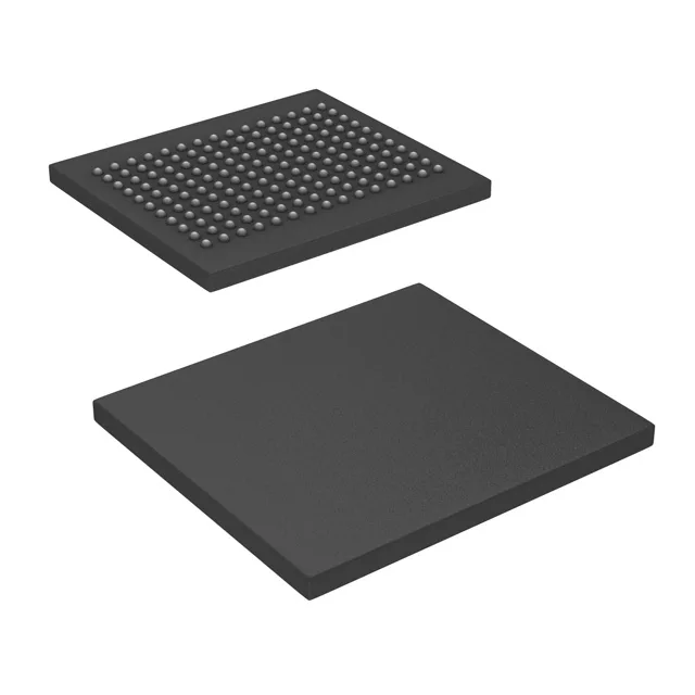
Cypress Semiconductor Corp CY7C1615KV18-333BZXC — Memory (DRAM / SRAM / Flash / EEPROM)

Cypress CY7C1615KV18-333BZXC QDR II SRAM, 144Mbit, 333 MHz

MPNCY7C1615KV18-333BZXC
Active

Cypress (Infineon) CY7C1615KV18-333BZXC, 144Mbit synchronous QDR II SRAM, 4M x 36 organization, 333 MHz clock, 1.7V–1.9V supply, 165-FBGA (15×17 mm) surface-mount, commercial 0°C to 70°C grade.

$296.1900Ref. price · indicative, final on quote
Independent supplier — new & surplus stockAuthenticity-screened · ESD-safe packingListing updated Jul 2026

Specifications

CY7C1615KV18-333BZXC specifications
ParameterValue
Memory typeVolatile
MountingSurface Mount
Supply voltage1.7V ~ 1.9V
Clock frequency333 MHz
Memory interfaceParallel
Operating temperature0°C ~ 70°C (TA)
PackageBulk
TechnologySRAM - Synchronous, QDR II
Memory size144Mbit
Memory formatSRAM
Case165-LBGA
Memory organization4M x 36

Product details

144 Mbit QDR II SRAM at 333 MHz — bus-fit for high-throughput buffers

The CY7C1615KV18-333BZXC is a 144 Mbit synchronous QDR II SRAM organized as 4M x 36 bits, clocked at 333 MHz over a parallel interface. The 333 MHz clock rate delivers a double-data-rate burst on both read and write ports.

Frequently asked questions

Can I use the CY7C1613 (8M × 18) or CY7C1625 (16M × 9) as a drop-in replacement for the CY7C1615 (4M × 36)?

No — the memory organization differs, so the address-to-data bus mapping is not compatible. Firmware written for the 4M × 36 device will not correctly access the 8M × 18 or 16M × 9 variants without source-level changes.

Does the higher-speed CY7C1650KV18-450BZC share the same interface map as the CY7C1615KV18-333BZXC?

Both parts share the 4M × 36 organization, so the address and data bus widths are identical. The CY7C1650 runs at 450 MHz versus 333 MHz — the higher clock rate is a timing-margin consideration, not a functional incompatibility.