What this NoBL SRAM does on the bus
It runs at a 167 MHz clock with a 3.4 ns access time, meaning the controller can start a new read or write on every clock edge without inserting dead cycles for bus turnaround — critical for high-throughput data buffers in networking switches, base stations, or FPGA-based signal processing pipelines. The 36-bit word width matches a 36-bit data bus directly, saving external byte-mux logic.
3.4 ns access at 167 MHz — timing closure note
The 3.4 ns access time at 167 MHz gives the memory controller a tight but workable setup window. Compared to the faster CY7C1470BV33-200AXC (3.0 ns at 200 MHz), this part trades top-end clock speed for slightly relaxed timing — useful if your FPGA or ASIC memory interface has marginal hold time on the fast corner. The 167 MHz clock aligns with many mid-range FPGA memory controllers without needing a PLL to divide down.
Package and temperature — board-level fit
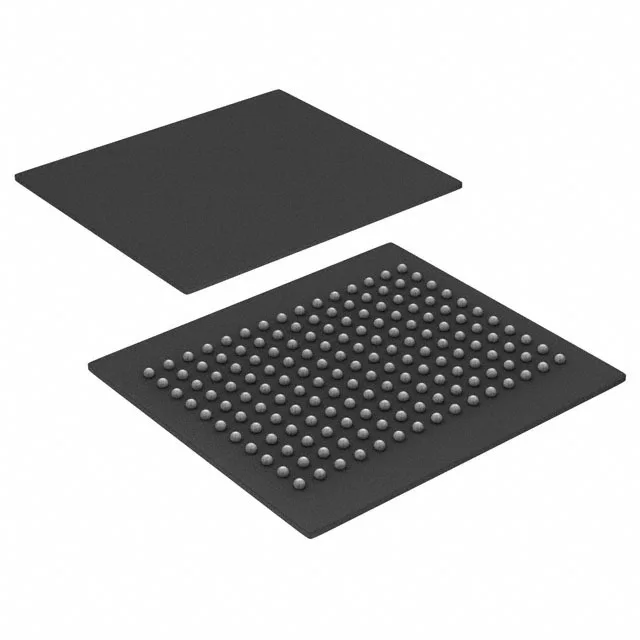
The 165-FBGA (15x17 mm) package requires controlled-impedance PCB layout and X-ray inspection post-reflow.