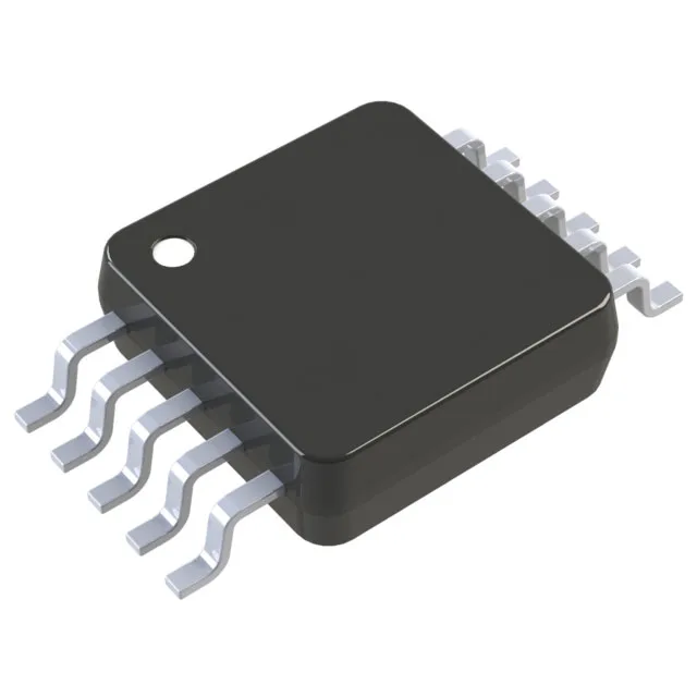
The MAX4253EUB+ comes in a 10-lead µMAX (also called uSOP) package — 3.0 mm body width, 0.5 mm pin pitch. The tube delivery means no tape-and-reel fee for low-volume builds, but the tube itself is non-reelable — plan for manual placement or a tube feeder on the pick-and-place line. Supply decoupling should sit within 2 mm of each supply pin — a 0.1 µF ceramic plus a 10 µF bulk cap per channel. The 0.5 mm pitch leaves little room for a via-in-pad; route the supply traces out on the top layer and drop vias outside the package footprint.
Slew rate and bandwidth — the signal ceiling
The full-power bandwidth — the frequency at which the output can swing rail-to-rail without slewing — is about 47 kHz for a 2 V peak-to-peak swing (slew rate / (π × Vpk)). Above that, the output distorts into a triangle wave. For a 100 mVpp signal, the usable bandwidth extends to roughly 950 kHz. Keep the closed-loop gain × bandwidth product under 3 MHz to avoid gain peaking.
Input bias and offset — sensor front-end fit
Input bias current is 0.1 pA typical — that is low enough to ignore for most applications, but it does double every 10°C above 25°C. At 85°C, expect roughly 6.4 pA. For a 1 MΩ source impedance, that bias current creates a 6.4 µV voltage error at the input — still small. The 70 µV input offset voltage, however, is the dominant DC error term. A nulling resistor in the feedback path or a trim pot on the offset-null pins (if available in the pinout) can zero it out, but for a single-supply 5 V system, 70 µV represents 0.0014% of the full-scale range — adequate for 12-bit resolution without calibration.
Runs on any single supply from 2.4 V to 5.5 V, or split supplies up to ±2.75 V. At 420 µA per channel (840 µA total for both), the quiescent power at 3.3 V is 2.8 mW — low enough for always-on sensor nodes. The 68 mA output drive per channel means it can directly drive a 32 Ω headphone load or a 100 Ω analog meter without a buffer stage.
ROHS3 compliant (lead-free, no restricted substances). No UL, IEC, or AEC-Q qualification is stated in the record.