8051 core at 25 MHz — what the clock rate means for throughput
The DS89C450-QNG+ runs an 8051 core at 25 MHz. Unlike some modern MCUs that execute one instruction per clock, the 8051 architecture uses 4 clock cycles per machine cycle, so the effective throughput is 6.25 MIPS at 25 MHz — not 25 MIPS. This matters for timing loops and UART baud-rate generation: a 1 ms delay loop counts 6,250 instruction cycles, not 25,000. The 64 KB on-chip Flash (64K x 8) holds the full firmware image without external memory for most applications. The 1K x 8 SRAM is the tight resource — a large call stack, multiple buffers, or a TCP/IP stack will overflow it. Budget the RAM before committing the BOM line.
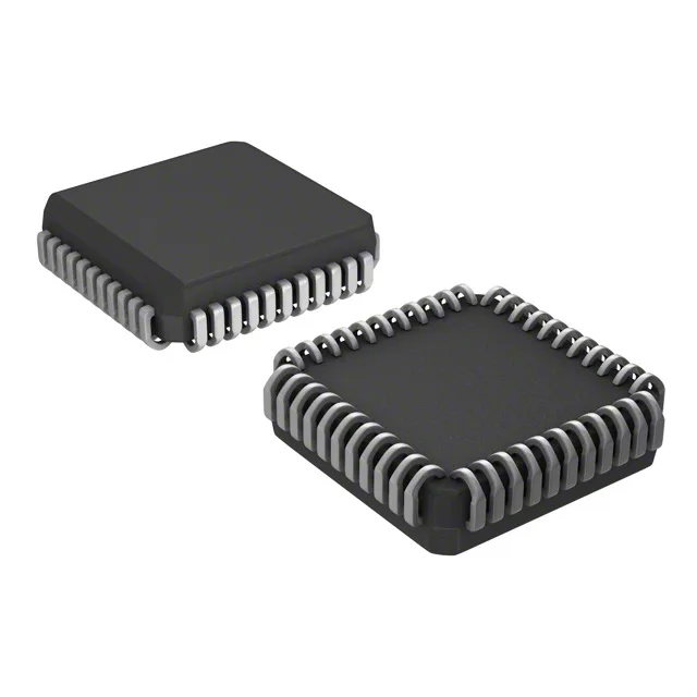
44-PLCC package — footprint and rework considerations
The 44-PLCC (J-lead) package measures 16.59 mm per side. J-leads are less common than gull-wing QFPs; the PLCC socket footprint differs from a soldered-down PLCC land pattern. If the design uses a socket, verify the socket's insertion force and the MCU's orientation key — the PLCC has a chamfered corner that must align with the socket's key. The I/O pins are 5 V-tolerant but not 3.3 V-compatible without a level translator.
Industrial temperature grade and on-chip supervision
This covers most factory-floor, outdoor telecom, and HVAC controller environments. It does not cover extended industrial (-40 to +105 °C) or automotive under-hood applications. The integrated power-fail reset and watchdog timer reduce external component count. The power-fail reset monitors the supply rail and holds the MCU in reset when Vcc drops below the threshold, preventing brownout corruption of the Flash or SRAM. The WDT resets the MCU if the firmware hangs — useful in unattended or safety-monitoring equipment.
Active lifecycle and sourcing posture
No pin-compatible second source or official successor is listed. The 8051 ecosystem has many alternatives, but a direct drop-in replacement from another vendor would require verifying the PLCC footprint, the oscillator circuit, and the peripheral register map — not guaranteed without a board spin.