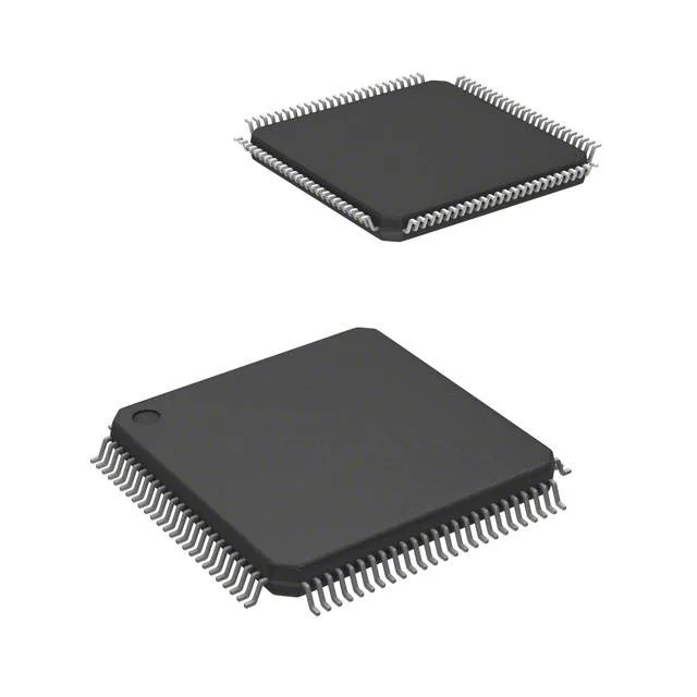
STMicroelectronics STM32F407VGT6 — Microcontrollers & Processors (MCU / MPU / DSP)

STM32F407VGT6 ARM Cortex-M4 MCU, 168 MHz, 1 MB Flash

MPNSTM32F407VGT6
Active

STMicroelectronics STM32F4 series, STM32F407VGT6, 32-bit ARM Cortex-M4 MCU, 168 MHz, 1 MB Flash, 192K x 8 SRAM, 100-LQFP (14x14 mm), -40°C to 85°C, 1.8V to 3.6V supply.

$7.83626Ref. price · indicative, final on quote
Packaging100-LQFP
RoHSROHS3 Compliant
SeriesSTM32F4
Independent supplier — new & surplus stockAuthenticity-screened · ESD-safe packingListing updated Aug 2026

Specifications

STM32F407VGT6 specifications
ParameterValue
SeriesSTM32F4
MountingSurface Mount
Oscillator typeInternal
Program memory typeFLASH
Voltage - supply (Vcc (Vdd))1.8V ~ 3.6V
Operating temperature-40°C ~ 85°C (TA)
Speed168MHz
PackageTray
RAM size192K x 8
Core size32-Bit Single-Core
PeripheralsBrown-out Detect/Reset, DMA, I²S, LCD, POR, PWM, WDT
ConnectivityCANbus, DCMI, EBI/EMI, Ethernet, I²C, IrDA, LINbus, SPI, UART/USART, USB OTG
Number of i (O)82
Core processorARM® Cortex®-M4
Case100-LQFP
Data convertersA/D 16x12b; D/A 2x12b
Program memory size1MB (1M x 8)

Product details

The 82 I/O pins and the peripheral set — Ethernet MAC, two CAN 2.0B interfaces, USB OTG HS/FS, twelve 16-bit timers, two 32-bit timers, three 12-bit ADCs (16 channels), and two 12-bit DACs — make it a single-chip gateway for industrial automation, motor drives, and networked embedded systems that need deterministic response and rich connectivity.

1 MB Flash and 192 KB SRAM — sizing the firmware and data buffers

The 1 MB Flash (1M x 8) is organized for firmware that includes a full RTOS, a TCP/IP stack, a file system, and application code without external memory. The 192 KB SRAM (192K x 8) supports multi-packet Ethernet buffers, CAN message queues, and real-time data acquisition. The Flash is rated for 10,000 erase/write cycles typical — adequate for field-update scenarios with wear-leveling in the bootloader.

100-LQFP (14x14 mm) — board-level integration check

Connectivity set — Ethernet, CAN, USB OTG, and serial interfaces

The STM32F407VGT6 integrates an Ethernet MAC (MII/RMII), two CAN 2.0B controllers, a USB OTG HS port (with ULPI for external PHY), a USB OTG FS port, three SPI, three I²C, four USARTs plus two UARTs, an IrDA transceiver, and a DCMI camera interface. This peripheral mix eliminates the need for separate interface ICs in many gateway, HMI, and data-logger designs. The DMA controller (16-stream, 8-channel) offloads peripheral-to-memory transfers without CPU intervention.

Frequently asked questions

Where can I buy STM32F407VGT6 with competitive pricing?

We source the STM32F407VGT6 through independent distribution channels and can provide a competitive quote against an RFQ.

What is the maximum speed of STM32F407VGT6?

The STM32F407VGT6 is rated for a maximum core clock of 168 MHz. At this speed, the ARM Cortex-M4 with FPU delivers 210 DMIPS and 1.25 DMIPS/MHz, suitable for real-time control and signal processing tasks.

What package is STM32F407VGT6 available in?

This order code is supplied in a 100-LQFP package with a 14x14 mm body and 0.5 mm pitch. It is a surface-mount tray-packaged device.

Can STM32F407VGT6 be used as a replacement for STM32F407VET6?

The STM32F407VET6 is a different density variant within the same STM32F407 family. The VGT6 carries 1 MB Flash and 192 KB SRAM; the VET6 typically has 512 KB Flash and 192 KB SRAM. They share the same 100-LQFP footprint and pinout, so a firmware image sized for 512 KB can run on the VGT6, but the reverse is not possible. Verify the Flash memory map and bootloader compatibility before substituting.